4.2. Carrier effective mass
4.2.1. Introduction
The effective mass is a suitable method to describe the density of states and electron transport on semiconductors and insulators materials [W05]. This approach is based on a free electron model and has been proven to be helpful to understand and engineering electronic materials [GRL17].
The effective mass values of the charge carriers are obtained from a free electron-like parabolic fit of band structure extrema. On NanoDCAL, these values are calculated by a finite-difference second order derivative of energy band (\(E\)) with respect to the electron momentum \(k\). The energy of the electron is expanded in a Taylor series around the extrema energy point \(k_{0}\):
The carrier effective mass \(m^{\ast}\) is expressed in unit of rest mass \(m_{0}\) of an electron as:
Since the effective mass is essentially related to the curvature of the dispersion relation, bands of large curvature correspond to small effective masses (light) while flatter bands are related with larger effective masses (heavier), as schematically show in Fig. 4.2.1
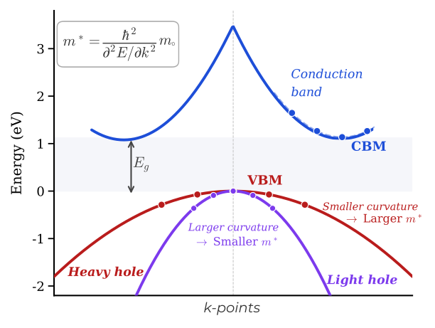
Fig. 4.2.1 Schematic band structure showing how band curvature determines the carrier effective mass: large curvature corresponds to light carriers, while flat bands correspond to heavy carrier.
To compute the effective mass using NanoDCAL code we have to perform the following steps:
Build the structure:
Generate the Si primitive cell using ASE.
Self-consistent (SCF) calculation:
Perform the ground state calculation.
Band structure calculations:
Calculate the band structure along high-symmetry k-points.
Effective mass calculation:
Calculate the carrier effective masses from the band curvature.
In the previous section (SOI), we already learned how:
Generate the Si crystal using ASE and the Python script
gen_Si.py(step 1);Generate and execute the SCF calculation using the Python script
gen_scf_nospin.py(step 2);Generate and calculate the band structure using the Python script
gen_bs_input.py(step 3).
From step 3, we can analyze the \(E-k\) diagram and choose the \(k\)-direction in which the effective mass will be calculated.
4.2.2. Effective mass calculation
Generating the effective mass input file
With the converged SCF solution in NanodcalObject.mat, we can generate the effective mass input file using the provided Python script gen_emass_input.py.
Generate the effective mass input file (EffectiveMass.input) by running:
python gen_emass_input.py
Effective mass input file
system.object = NanodcalObject.mat
calculation.name = effectiveMass
calculation.effectiveMass.massParameters = {'hole',-1,1,[0 0 0],[1/2 1/2 1/2],;'electron',1,1,[0 0 0],[1/2 0 1/2]}
The keywords specify the following:
system.objectIf it is not empty, the system is defined by the input object. In this case, all other parameters related to the system in the input file will not be used.calculation.nameThe description must be provided to invoke the kind of calculation.calculation.effectiveMass.massParameters. The user should set:The charge carrier: hole or electron.
The energy band information or band index, where: 1 represents the bottom of the conduction band, 2 represents the sub-conduction band; -1 represents the top of the valence band, and -2 represents the sub-valence band.
The spin information, where 1 represents spin-up and 2 represents spin-down. For NoSpin or GeneralSpin calculation, this value is 1.
The \(k\)-points coordinates (represented by fractional coordinates), used to define the \(k\)-path.
Important
NanoDCAL will compute the band structure along the \(k\)-path, find the minimum (for electrons) and maximum (for holes), and perform a quadratic fit at the extremum. The quadratic fit is performed along the \(k\)-direction set by the \(k\)-path and its two transverse directions, which means that the charge carriers effective masses will be also calculated along those directions.
Tip
The Python script gen_emass_input.py accepts parameters for different band indices and \(k\)-paths. The user can modify the script arguments to customize the effective mass calculation for different materials and \(k\)-directions.
Running the effective mass calculation
Run the simulation with the EffectiveMass input file:
nanodcal EffectiveMass.input
After the calculations, the .mat data files can be loaded in MATLAB platform to extract the effective mass results.
4.2.3. Effective mass for Si
The output file has the following information:
The calculated results for effective mass of electrons (\(m^{\ast}_{n}/m_{0}\)) and holes (\(m^{\ast}_{p}/m_{0}\)) will be localized at the first and second lines of the output file, respectively;
For each band index, three masses are written in the output. These three masses are the eigenvalues of the effective mass tensor.
In this example, silicon has anisotropic effective masses for electrons and holes. The following discussion will be based on the band structure plot of silicon crystal, which can be viewed here.
Tip
In this example the effective mass calculation was performed for several band indices. The user should modify the \(k\) path and band index according to the system.
Valence band masses (holes)
The highest occupied state (valence band maximum) is localized at the \(\Gamma\)-point. Thus, the corresponding effective masses of holes were calculated between \(\Gamma\)-point [0 0 0] and \(L\)-point [1/2 1/2 1/2]. The three-fold degenerated valence bands are indexed as:
Heavy-hole (HH) for band indices -1 and -2;
Light-hole (LH) for band index -3.
The calculated hole effective masses are showed below:
band index |
effective mass |
mass_l |
mass_t1 |
mass_t2 |
|---|---|---|---|---|
-1 |
HH |
0.684 |
0.776 |
2.481 |
-2 |
HH |
0.684 |
0.394 |
0.266 |
-3 |
LH |
0.098 |
0.107 |
0.111 |
Note
The mass_l was calculated along the longitudinal \(k\) path direction.
The mass_t1 was calculated along the first transverse direction
The mass_t2 was calculated along the second transverse direction
Conduction band masses (Electrons)
The lowest unoccupied band appears along the \(\Gamma\)-point [0 0 0] and \(X\)-point [1/2 0 1/2], around \(0.85X\). The electron effective mass eigenvalues are presented below:
band index |
effective mass |
mass_l |
mass_t1 |
mass_t2 |
|---|---|---|---|---|
1 |
electron |
0.9262 |
0.194 |
0.194 |
4.2.4. Density of states effective mass
The occupation of electrons in a solid is defined by the Fermi surface, which is a direct consequence of the Pauli exclusion principle. The density of state effective mass (\(m^{*}_{dos}\)) essentially maps the volume of the Fermi surface and affects the Seebeck coefficient calculation. So, for a semiconductor material the description of \(m^{*}_{dos}\) is of paramount importance.
The \(m^{*}_{dos}\) is related to the diagonal elements of the mass tensor (\(m_{1}\), \(m_{2}\), and \(m_{3}\)). Most of the band structures from semiconductors have ellipsoidal energy surfaces, resulting in different longitudinal (\(m^{*}_{l}\)) and transversal (\(m^{*}_{t}\)) effective masses. The density-of-states effective mass is expressed as:
where \(M_{c}\) is the number of equivalent band minima.
The density-of-states effective mass for Si
For instance, the silicon possess 6-fold valley degeneracy (\(M_{c}=6\)), with two equivalent directions (the transverse direction) and one longitudinal direction. The \(m^{*}_{dos}\) value for silicon was calculate to be:
4.2.5. Conductivity effective mass
The material conductivity is inversely proportional to the effective masses. In this case, a simple conductivity effective mass \(m^{*}_{C}\) could be defined to estimate the electron mobility of semiconductor materials. The conductivity due to multiple band maxima or minima is proportional to the sum of the inverse of the individual masses multiplied by the density of carriers in each band. The resulting effective mass \(m^{*}_{C}\) expression is given by:
The effective mass for conductivity in Si
For silicon crystal, we found
Important
The carrier effective mass analyses for silicon could be improved if spin-orbit effects were taken into account. The user should be able to modify the input files and repeat the calculations to improve accuracy of these results.
4.2.6. References
A. L. Wasserman. Effective masses J. Phys. Condens. Matter. (2005) p. 1-5.
Z. M. Gibbs, F. Ricci, G.g Li, H. Zhu, K. Persson, G. Ceder, G. Hautier, A. Jain, G. J. Snyder. Effective mass and Fermi surface complexity factor from ab initio band structure calculations npj Comput. Mater. 3, (2017) p. 1-8.