NEGF-DFT in NanoDCAL
In nanodcal, quantum transport calculations are done by a combination of the Keldysh non-equilibrium Green’s function (NEGF) and a self-consistent field theory (SCF). The SCF theory is based on a Hamiltonian that looks like DFT, namely having terms of kinetic energy, Hartree potential, exchange-correlation potential, potential due to atomic cores and other external potentials. These potentials even have the same form as the DFT, but the electronic density that enters these potentials is calculated at non-equilibrium by NEGF, and not calculated at equilibrium by Eq. (15). In addition, since there is no variational principle at non-equilibrium, the equations of NEGF-SCF theory is not solved by total energy minimization like in DFT, but by direct solution of the Hamiltonian (albeit still self-consistently). Therefore, the NEGF-SCF theory is qualitatively different from the equilibrium and ground state DFT. In other words, NEGF-SCF is not a ground state theory because it is determined by a non-variational and non-equilibrium density matrix. In the literature [TGW01], the NEGF-SCF method was however given the name of NEGF-DFT because the SCF procedure looks like that in DFT. But one should realize that the “DFT” in NEGF-DFT is qualitatively different, even though it has terms in the NEGF-DFT Hamiltonian similar to the equilibrium DFT. From now on, we shall adapt the name NEGF-DFT with the above understanding in mind. Whenever refereed separately, “DFT” is reserved for the conventional equilibrium ground state density functional theory, while “DFT-like” is for the self-consistent field theory in NEGF-DFT.
The basic computational idea behind the real space NEGF-DFT approach is to determine the Hamiltonian and electronic structure of the system by a DFT-like self-consistent field theory, calculate the non-equilibrium density matrix by NEGF, and account for the open transport boundary conditions and electrostatic potential boundary conditions (due to external bias or gate voltages) by real space numerical techniques. The input to a NEGF-DFT calculation is the atomic structure which can be determined using other methods, and the output of NEGF-DFT is quantum transport properties of the atomic structure as well as many other physical quantities.
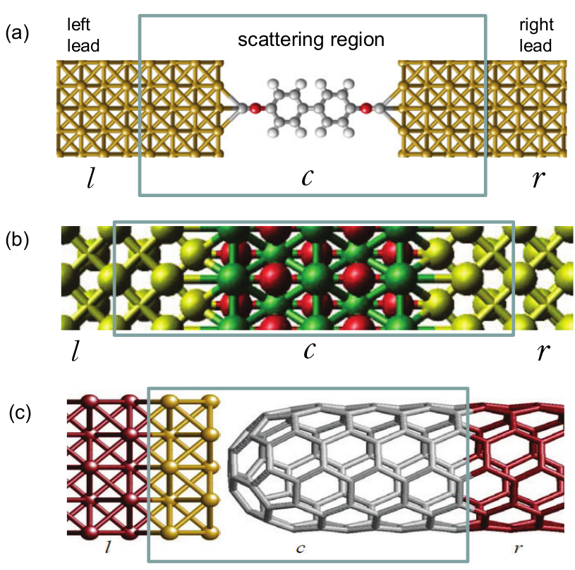
Fig. 14 Schematic of two-probe devices along the transport (z) direction. The central box indicates the device scattering region C that includes the scatterer plus a few layers of electrode atoms. The left and right electrodes (leads) extend to \(z=\pm\infty\). (a) A molecular transport junction where electrodes have a finite cross-section; (b) A solid state Fe/MgO/Fe magnetic tunnel junction which is periodic in the transverse x,y directions; (c) A gold-nanotube tunnel junction where the left and right electrodes are made of different atoms.
We use the two-probe open transport junctions shown in Fig. 14 as an example for our discussions. Similar discussions can be easily extended to multi-probe structures. Fig. 14 (a) is for a molecular transport junction where a molecule is sandwiched between two gold electrodes having a finite cross section; Fig. 14 (b) is a solid state magnetic tunnel junction where two Fe metal sandwich a MgO tunnel barrier, and the device is periodic in the transverse x,y directions (transport is in the z direction). The device is divided into three sections: the central scattering region plus the two electrodes. The scattering region must include several layers of the electrode atoms, as shown. The device electrodes or leads extend to \(z=\pm\infty\) where bias voltages are applied and electric current collected. The electrode is thus a semi-infinite structure and it provide the transport boundary conditions: for instance electrons come from the left electrode, scatter at the central scattering region, reflect or transmit to the right electrode. Quantum transport is therefore a scattering problem by the potentials in the scattering region. NEGF-DFT method calculates these potentials self-consistently before predicting the final transport properties.
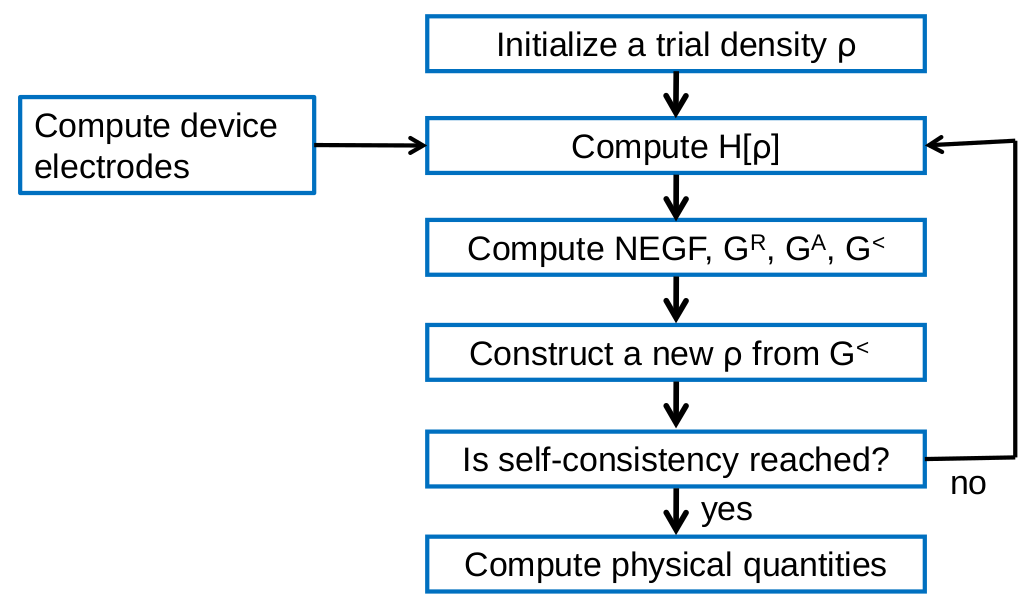
Fig. 15 Flowchart of the self-consistent cycle in the NEGF-DFT calculation.
The flowchart of NEGF-DFT is shown in Fig. 15. Compare with Fig. 13, there are major differences. First, since NEGF-DFT is mainly used to deal with quantum transport in open devices, there are device electrodes to deal with. Second, the density matrix is calculated at non-equilibrium by NEGF and not from the Kohn-Sham wave functions as in Eq. (15). In steady-state quantum transport, the driving force of the non-equilibrium condition is the finite external bias voltage applied to the electrodes such that a current is driven to flow through the device. The primary application of nanodcal is to predict the non-equilibrium steady-state quantum transport, even though the output of nanodcal can be used to construct further analysis of time dependent phenomena such as to calculate the frequency dependence conductance. Finally, compared with the conventional DFT, there are numerical and implementation differences on many parts of the NEGF-DFT calculation procedure. This section presents the NEGF-DFT method within nanodcal.
Before go into the details, we emphasize (will also become clear below) that NEGF-DFT reduces to the equilibrium ground state DFT in the limit of zero external driving force, as it should be [TGW01]. There are also extensive discussions in the literature on fundamental issues concerning this formalism. Our view is that for non-equilibrium quantum transport, a most important qualitative physical consideration is the non-equilibrium statistical information of the device scattering region: notably it is not Fermi-Dirac and must be calculated by NEGF. Next, a quantitative consideration is the device Hamiltonian which affects the level of quantitative accuracy and predictive power of the theory. In the history of charge transport theory, Hamiltonian at the level of classical particle interaction, the effective mass approximation, the \({\bf k\cdot p}\), Poisson-Schrodinger equations, tight binding potential, and DFT-like theory have all been widely used. Some higher level Hamiltonian has also been tried but their computational loads are often prohibitively large. In this list of possible Hamiltonian, DFT-like theory provides a good compromise between practicality and accuracy, and DFT has indeed been the de facto standard method in materials theory. It is therefore natural to combine NEGF with the DFT-like theory which is what nanodcal does. The ultimate power of the NEGF-DFT formalism is its predictive nature, e.g. no phenomenological parameters are needed. It has also been applied to large number of practical device modeling problems that compare rather consistently with the corresponding measured data.
Calculating the electrodes
In Fig. 14, the semi-infinite electrodes (leads) play several rolls. First, they guild the incoming electron waves (Bloch waves of the electrodes) to the device scattering region. Second, they provide the electro-static boundary conditions of the Hartree potential of the scattering region. Third, they provide self-energies to the Hamiltonian of the scattering region.
A device lead consists of super-cells of the lead atoms, repeating into a semi-infinite structure. Practically, since we always include several layers of the lead atoms inside the scattering region C (see Fig. 14), on either side of the lead-central boundary, the atoms see the same potential. Therefore, nanodcal calculates the electrode Hamiltonian by DFT assuming the electrodes are infinitely long. After the calculation, nanodcal cuts the infinite lead to a semi-infinite lead, stores the potential of the lead’s surface \(V_{s}(x,y)\) where subscript \(s\) is the z-coordinate of lead-central boundary. For transport, leads are in the metallic regime or they are made of metals, therefore leads are at equal potential after a voltage is applied to them. In order words, if a bias voltage is applied to a lead, the lead’s potential is simply a rigid shift by the bias from its original potential value. Hence, having bias or not, the lead’s Hamiltonian is calculated using the conventional DFT and nanodcal uses that described in Chapter 2 for this purpose.
After the self-consistent DFT is converged, \(V_{s}(x,y)\) as well as the Hamiltonian and overlap matrix elements of Eq. (28) in Section DFT in NanoDCAL are stored for further use.
Hartree potential of the central region
According to Fig. 15, after the device leads are calculated, we move to solve the Hamiltonian of the central scattering region of the device. Consider bias voltages \(V_{l}\) and \(V_{r}\) are applied to the left and right leads in Fig. 15 respectively, which shift the corresponding potential of the leads by these values. The potential difference \(\Delta V=V_{l}-V_{r}\) is dropped at the scattering region. Therefore, nanodcal solves the Hartree potential from the Poisson Eq. (2) subjecting to the following boundary conditions:
where the left hand side is the Hartree potential \(V_{{ H}}\) of the scattering region at the lead-central interface which is located at \(z=z_{S}\) (see Fig. 14); the right hand side is the Hartree potential of the lead at the same lead-central interface, calculated in the above section. In DFT-like mean field theory, once the Hartree potential is matched at the boundary, the charge density will automatically match there. Importantly, in order for Eq. (32) to be valid, the central region must include a number of buffer layers of the lead atoms as shown in Fig. Fig. 14. How many buffer layers are suitable depends on the problem and the material of the leads. For metallic leads such as gold, four layers are likely adequate. To be sure, one can calculate transport properties for different buffer layers and compare the results.
Self-energy of the leads
For open systems like those in Fig. Fig. 14, there are infinite number of electrons in the semi-infinite device leads which interact with the charges in the central scattering region. In other words, our system is infinitely large. After dividing the system into a central scattering region plus the leads as shown in Fig. Fig. 14, there are finite degrees of freedom in the central region but still infinite large number of degrees of freedom in the leads. In the NEGF-DFT approach, the contribution of any electrode \(\alpha\) is integrated out to produce a self-energy \({\mathbf \Sigma}_{\alpha}\) that enters the Hamiltonian of the central region. The details of this procedure can be found in Ref. [Datta, TGW01].
Using the LCAO basis Eq. (16), \(\Sigma_{\alpha}\) becomes a matrix. \(\Sigma_{\alpha}\) is also a function of electron energy \(E\) and possibly momentum \(\textbf{k}\) for periodic systems, and every lead contributes its own self-energy to the central region. Thus, for example, the total self-energy for a two-probe system is \(\Sigma=\Sigma_{l}+\Sigma_{r}\).
Taking into account the self-energy from the leads, the matrix Eq. (27) becomes:
where summation over \(\nu^{\prime}\) is implied; \(E\) is the electron energy and \(G_{\nu^{\prime}\nu}^{E}\) is the Green’s function matrix to be solved (see below).
It turns out that \(\mathbf{\Sigma}_{\alpha}\) is related to the surface Green’s function of the semi-infinite lead \(\alpha\). There are well known methods to calculate the surface Green’s function for semi-infinite but otherwise periodic structures. Both iterative and direct solutions were published in the literature [SSR84,BL99_].
Calculating the Green’s functions
The next step in Fig. 14 is to calculate the Green’s functions. For a discussion on some fundamentals of Green’s functions for transport, we refer readers to several excellent books [Datta, HJ98]. Practically, nanodcal calculates the Green’s functions from Eq. (33) by inverting the matrix,
where the superscripts \(R,A\) indicates the retarded and advanced quantities, respectively. Using the fact \({\bf G}^{A}\ =\ \left({\bf G}^{R}\right)^{\dagger}\), nanodcal computes \({\bf G}^{R}\) from this equation by inverting the matrix of the right hand side.
Various advanced algorithms have been implemented in nanodcal to most efficiently invert the matrix. So far, nanodcal has implemented a block diagonal matrix structure and achieves linear scaling — O(N), along the transport direction. This is adequate for most transport problems where the device is long in the transport direction but thin in the other transverse directions, as those shown in Fig. 14. For systems which are both long and very thick, the matrix problem becomes the computational bottleneck.
Once \({\bf G}^{R,A}\) are obtained, nanodcal calculates the Keldysh NEGF \({\bf G}^{<}\) from the Keldysh equation [HJ98, TGW01]:
where
where \(f_{\alpha}\) is the Fermi function of lead-\(\alpha\); and \(\Gamma_{\alpha}\) is the linewidth function of the same lead, given by
Note that Eq. (36) is justified for mean field theory in the central scattering region of the device. If there are strongly correlated physics in the central region, more advanced \(\Sigma^{<}\) is necessary and users of nanodcal can supply a calculator for that purpose.
Calculating \(\rho\) from \({\bf G}^{<}\)
Moving on to the next step in Fig. 14, we calculate the density matrix \(\hat{\rho}\) and real space charge density \(\rho(\textbf{r})\) from \({\bf G}^{<}\). Note that in conventional ground state DFT, \(\rho(\textbf{r})\) is calculated from Eq. (15). But in NEGF-DFT, \(\rho(\textbf{r})\) is calculated by NEGF through the non-equilibrium density matrix \(\hat{\rho}\), namely,
The density matrix \(\hat{\rho}\) is a matrix in the LCAO orbital space. Its real space form is calculated by using the LCAO basis functions Eq. (16), namely,
where \({\bf r}\) is associated with orbital \(\zeta_{\mu}\) and \({\bf r'}\) with \(\zeta_{\nu}\). Finally, the charge density is the diagonal elements of the density matrix, namely
Practically, it is very difficult, if not impossible, to carry out the integration in Eq. (38) numerically. Further manipulations are done for its calculation. First, the upper limit is truncated to the chemical potential of the right lead \(\mu_{r}\) (we assume \(\mu_{r}>\mu_{l}\). Second, for energy \(E<\mu_{l}\), all the energy levels of the scattering region are occupied at low temperature, namely any statistical information is lost and Eq. (38) is reduced to the following formula [TGW01],
Importantly, the \({\bf G}^{R}\) in the first term on the right hand side is analytic on the upper half of the energy plane, hence the first integral can be very accurately calculated using a complex contour in the upper half plane. The poles of \({\bf G}^{R}\) are near the real energy axis but in the lower half energy plane. For the second integral of Eq. (41), unfortunately it can only be calculated along the real energy axis since \({\bf G}^{<}\) is not analytic on both the upper and the lower planes. Fortunately, for practical situations the integration range (called the bias window), \(\mu_{l}\rightarrow\mu_{r}\), is not very large and is basically provided by the external bias voltage.
The integrals of Eq. (41) are discretized and numerically computed. Fig. 16 shows the contour of nanodcal. At a finite temperature \(T\), the integration limits are smeared by a few \(k_{B}T\) where \(k_{B}\) is the Boltzmann constant, and Fermi poles appear on the imaginary energy axis which are taken into account by calculating the residues.
Self-consistency and calculation of Hamiltonian
Having calculated the real space charge density from Eqs. (41), (40), the next step in Fig. 14 is to check if self-consistency is reached. If it is, we move forward to calculate physical quantities. It is not, we have to continue the SCF iterations. As discussed in the last paragraph of Section Solution of the KS equation, a number of schemes has been implemented in nanodcal to mix charge density or other quantities such as potentials or mixtures of these quantities, along the SCF iteration path.
From the real space charge density \(\rho(\textbf{r})\), the Hamiltonian of the device scattering region is calculated using the formula in Chapter 2. In particular, \(\rho(\textbf{r})\) is used in Eq. (2), together with the transport boundary condition Eq. (32), to calculate the Hartree potential. Another potential that needs \(\rho(\textbf{r})\) is the exchange-correlation potential \(V_{xc}=V_{xc}\left[\rho(\textbf{r})\right]\) in Eq. (29). Several particular functional forms of \(V_{xc}\) on \(\rho(\textbf{r})\) can be found in nanodcal, including LDA, LSDA, and various GGA. A user can also supply his/her own \(V_{xc}\) to nanodcal using the API. Apart from the effective potential \(V_{eff}\) of Eq. (29), other terms of the Hamiltonian do not depend on \(\rho\) and are calculated outside the SCF iteration loop. These rigid atomic fields and their matrix elements are calculated only once by Eq. (30).
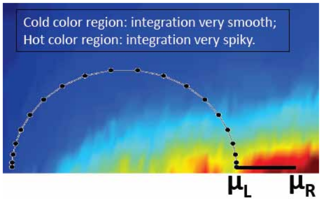
Fig. 16 A typical contour map for calculating the non-equilibrium density. The complex contour starts from a very large negative energy at least two Rydbergs below the band bottom of the device electrodes. The hotter the color, the more spiky the integrands. In nanodcal, the complex contour can also be divided into more segments each having different number of points for better numerics. For the integration over the bias window, \(\mu_{l}\rightarrow\mu_{r}\), direct computation on the real energy axis is done.
Datta, Electronic Transport in Mesoscopic Systems, (Cambridge University Press, New York, 1995).
Taylor, J., Guo, H., & Wang, J. (2001). Ab initio modeling of quantum transport properties of molecular electronic devices. Physical Review B, 63(24), 245407.
Waldron, D., Timoshevskii, V., Hu, Y., Xia, K., & Guo, H. (2006). First Principles Modeling of Tunnel Magnetoresistance of Fe/MgO/Fe trilayers. Physical Review Letters, 97(22), 226802.
Lopez Sancho, M. P., Lopez Sancho, J. M., & Rubio, J. (1984). Quick iterative scheme for the calculation of transfer matrices: Application to Mo (100). Journal of Physics F: Metal Physics, 14(5), 1205–1215.
Bratkovsky, A. M., & Lambert, C. J. (1999). General green’s-function formalism for transport calculations with (formula presented) hamiltonians and giant magnetoresistance in co- and ni-based magnetic multilayers. Physical Review B - Condensed Matter and Materials Physics, 59(18), 11936–11948.
Haug and A.-P. Jauho, Quantum Kinetics in Transport and Optics of Semiconductors, (Springer-Verlag, New York, 1998).