Open Surface Calculations
There are many research problems that involve electronic structure of surfaces. Most commonly, a surface calculation is done using the slab geometry. Fig. 10 (a) plots a slab geometry of a Si surface. The slab is periodic in x-y directions but not in the z direction because the surface breaks translational symmetry. In a slab calculation, one surrounds the slab by vacuum regions. The bottom (left most layer in Fig. 10 (a)) layer of the slab must be saturated by hydrogen atoms to remove dangling bonds. To make sure the bottom layer does not interact with the top surface through the slab, enough layers must be included into the slab as indicated by \(L\) of Fig. 10 (a). For metal surfaces, it is not uncommon to use \(\sim L=20\) layers in the slab in order to guarantee accuracy. The entire supercell thus includes the slab, the vacuum region and the saturating H atoms. Using the supercell one can carry out a crystal calculation as shown in section Crystals.
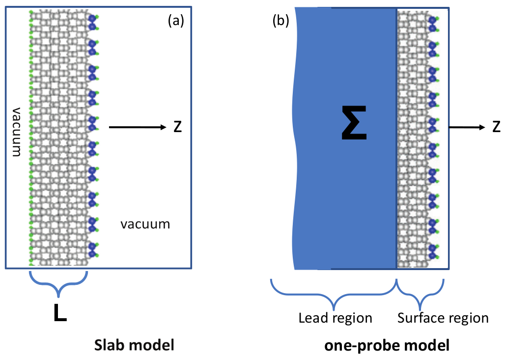
Fig. 10 Side view of a Si surface. (a) A typical supercell in slab geometry to represent the right most surface. The slab has thickness L and is surrounded by vacuum to isolate the slab from its periodic images. The left most layer of the slab is saturated by H atoms. (b) The one- probe representation which is a semi-infinite geometry starting from the surface and going to \(z = −\infty\). The semi-infinite geometry is divided into a surface region containing a few atomic layers, plus a lead region. In Green’s function theory, the lead region contributes a self-energy \(\Sigma\) to the Hamiltonian of the surface region.
In addition to the slab calculation of Fig. 10 (a), NanoDCAL also allows one to calculate open surfaces with infinite number of layers beneath the surface. This is the one probe capability which is explained in this section. Fig. 10 (b) plots the one probe geometry. Using this capability, one does not need very big vacuum regions as that in Fig. 10 (a) - as long as no atomic orbital extends out of the right most computation box boundary (see Fig. 10 (b)). There are no saturating H atoms needed because the one probe geometry half fills the space and is a semi-infinite system. The trick that reduces a semi-infinite system into something calculable is through the self-energy \(\Sigma\) shown in Fig. 10 (b), and by using the Green’s function approach. In the Theory section, these theories are explained in more detail. We have also seen \(\Sigma\) in section Two Probe Devices for two probe transport calculations.
A more important reason to consider the open surface geometry is for realistic device simulations. In fact, most electronic devices are fabricated on top of some substrates. At nanoscale, the effect of substrate to quantum transport through nanostructures sitting on the substrate, can be very important. Hence, if one wishes to consider a two probe device anchored on a solid state insulating substrate, one may use the open surface method of this Section to drastically reduce the system sizes.
Self-energy
In an one probe open surface calculation, the semi-infinite system is divided into two regions, the surface region that includes the surface layer plus a few layers underneath, and the bulk atomic layers underneath the surface region going all the way to \(z=-\infty\). The atoms in the bulk region provide a potential \(\Sigma\) to the surface region shown in Fig. 10 (b). Hence, as far as the surface calculation is concerned, the semi-infinite system becomes the surface region plus \(\Sigma\). This is exactly what we have done to reduce the electrodes of two probe devices in Section Two Probe Devices. In the Green’s function theory, what we have done is to integrate out the degrees of freedom in the semi-infinite bulk region whose effects to the surface region are provided by \(\Sigma\). Therefore, once \(\Sigma\) is obtained the actual DFT computation box only includes the surface region, although now the potential in the Kohn-Sham equation has a term \(\Sigma\).
The calculation procedure of \(\Sigma\) has already been discussed in Two Probe Devices and is shown schematically in Fig. 9 where the semi-infinite bulk region is divided into infinite number of identical principle layers (PL) each has width \(t\). In NanoDCAL, \(t\) is required to be thick enough so that a PL has direct orbital overlap only with its nearest neighbour PL. The box containing the surface region should also have enough layers so that atomic orbitals in PL-1 does not extend to the right of the surface.
An example
Let’s go to /example/Group3_Ag_OneProbe/ directory which has two
subdirectories, a /lead and a /system. The example is about the
calculation of electronic structure of Ag surface using the one probe
open surface feature of NanoDCAL. There is nothing special about the
lead calculation and we shall thus go to the system calculation
directly. In /system, please open the scf.input file, the essential
lines are the following:
calculation.name = scf
system.objectOfLead1 = ../lead/NanodcalObject.mat
system.numberOfLeads = 1
system.typeOfLead1 = ‘left’
system.voltageOfLead1 = 0
system.numberOfGates = 1
system.typeOfGate1 = ‘right’
system.voltageOfGate1 = -4.74
Line 2 tells NanoDCAL that the lead region has been calculated and the object file is in the directory just above the present one. Lines 3,4 tells nanodcal that lead 1 is the bulk region of the open surface which has zero applied voltage. Clearly you can add a voltage on the lead as well. Lines 6-8 are very important, they tell NanoDCAL that at the far end to the right, there is a gate, and a gate voltage of -4.74V is applied there. This gate voltage is nothing but the experimental work function of Ag.
In any one probe calculation, far from the open surface in the vacuum region, the potential should reach the vacuum level. For a perfect crystal surface, the energy needed to move an electron from the Fermi level to the vacuum level is the work function. Hence by setting the far-end boundary condition to be that of the work function, provides a good handle to the electrostatics during the SCF calculation. If one does not know the work function, then the gate voltage above should be adjusted so that one finds the ground state. Since work functions of most systems are known experimentally, they provide a good starting point.
Summary
The open surface capability provides a different way to analyze surfaces than the slab supercell calculation method commonly seen in surface science. More importantly, it provides a potential capability for investigating quantum transport of nanostructures that anchor on surfaces.