Two Probe Devices
The quantum transport model in NanoDCAL is discussed in Section 1.1 of the Theory section. Several atomic structures of two-probe transport junctions are plotted in Fig. 14 of the Theoretical Background. In this Section, we use an example to illustrate a two-probe quantum transport calculation. Schematically, a two-probe transport junction is plotted in Fig. 7 which is divided into three regions: the left and right leads as well as the central scattering region. Since the leads are semi-infinitely long, a two probe system is an infinitely large but non-periodic structure. Its calculation requires rather different method than those for molecule and crystal calculations.
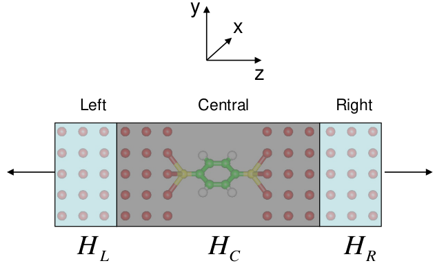
Fig. 7 The two-probe geometry representation of transport junction. The system is divided into three regions; the left/right leads and the centre scattering region. The leads extend to $z=pm infty$ and are made of infinite number of identical principle layers (PL), each PL has thickness $t$ which is large enough so that a PL only has direct orbital overlap with its nearest neighbour PL. The effect of all the PL to the center region is calculated by Dyson’s equation to give the self-energies $Sigma_l$ and $Sigma_r$ that are added to the Hamiltonian of center region. The center region contains several layers of the lead atoms.
In particular, after the atomic structure is prepared, a two-probe
calculation consists of three steps: (i) calculate the Hamiltonian of
the leads using DFT; (ii) calculate the Hamiltonian of the centre
scattering region using NEGF-DFT; (iii) post-analysis. Let’s use the
example of a two probe calculation in the /examples/Group10/Au-BDT-Au/
directory of NanoDCAL to illustrate how to carry out a transport
analysis. In this problem, we wish to calculate charge transport through
a benzenedithiol (BDT) molecule contacted by two gold electrodes.
Calculating the leads
In the NEGF-DFT calculations of the open device structure, from the computation point of view, the infinite system becomes the device scattering region plus the self-energies \(\Sigma\) (see below) due to the device leads. The first step is to calculate the electronic structure of the device leads which is considered to be a perfect crystal. Its electronic structure and potential serve as inputs to the two-probe device calculation, as shown in Fig.4 of the Theory. Since a lead is a periodic bulk structure, it is calculated in exactly the same way as a crystal calculation, already discussed in Section Crystals.
Go to the /examples/Group10/Au-BDT-Au/lead/ subdirectory of NanoDCAL
which contains two files, lead.xyz and scf.input. The lead.xyz is the
position file of the atoms in the supercell for a gold lead, in our
example it contains 36 gold atoms. The 36-atom supercell is periodically
extended to form a three dimensional gold crystal. The (111) direction
of this lead is oriented along the z-axis.
The input file scf.input is shown in Au lead input.
Comparing it to Fe scf input in Section
Crystals which is for a bulk DFT calculation, we immediately
realize that the lead calculation is precisely a bulk calculation. In
this particular example, all the lengths are in atomic unit (Bohr) by
line-4 of Au lead input.
system.name = Au.Lead
system.spinType= NoSpin
calculation.name = scf
calculation.control.lengthUnit= Bohr
system.centralCellVectors= [16.721242,19.307964,13.652799]
system.atomFile= lead.xyz
system.orbitalType= DZP
calculation.realspacegrids.number= [80,96,68]
calculation.k_spacegrids.number= [6,5,8]
calculation.occupationFunction.temperature= 50
calculation.SCF.maximumSteps= 100
calculation.SCF.mixer.class= cMixerBroyden
calculation.SCF.mixer.parameter.beta= 0.05
calculation.SCF.mixer.parameter.maxhistory= 9
In the bulk calculation example of Section Crystals, the supercell vectors were set by line-4 of Fe scf input, namely:
system.centralCellVectors = eye(3)*5.2202
which uses the Matlab function eye(3) to set up a \(3 \times 3\) identity matrix, and then multiply it by 5.22 au. In the gold lead example here, we set up the supercell in line-5 of Au lead input:
system.centralCellVectors = [16.721242,19.307964,13.652799]
For the present example which involve periodic three-dimensional leads, these values guarantees periodicity. The principle for a bulk calculation is to make sure that the supercell can periodically extend to all the dimensions correctly. How did we arrive at the above numbers? In the present specific example, the lead’s supercell has more than two layers and the layer-layer distance is the same. Let’s check that the supercell length in the z-direction, \(L_z = 13.652799\), is correct. Opening up the file lead.xyz, you will find positions of the 36 gold atoms: along the z direction these atoms locate at three layers hence there are only three different z-coordinates: \(z_1=2.275461\), \(z_2=6.826394\), and \(z_3=11.377327\). Clearly, the supercell length along the z-direction is the difference between \(z_1\) and \(z_3\) plus a layer-layer distance. The layer-layer distance along the z-direction can be obtained as \(b_z = z_2-z1=4.550933\). We thus obtain \(L_z =z_3-z_1+b_z=13.652799\), which is the value in the above cell vector. To obtain \(L_x=16.721244\), we do exactly the same. In lead.xyz, you can find that there are six equal-spaced layers along the x-direction, with coordinates \(x_1=0.5\), \(x_2=3.286874, \cdots\), and \(x_6=14.434368\). We obtain \(b_x=x_2-x_1=2.786874\) and, therefore, \(L_z=x_6-x1+b_x=16.721242\) which is the value in the above cell vector. Finally, one can obtain the value of \(L_y\) in exactly the same way.
It is the user’s responsibility to set up these values so that a bulk periodic calculation can be correctly done for the lead calculation. As already discussed in Section Crystals, even if one made a mistake in setting up these cell vectors, NanoDCAL would still run. As a diagnostic, NanoDCAL always outputs the system it determines to be, in this case there is a line in the standard output (Matlab command window) which reads as:
System Type: periodic-3D, no spin
This output line tells us that NanoDCAL is running a none
spin-polarized periodic 3-dimensional structure, which is indeed what we
set out to do. If one of the cell vectors was set up incorrectly, you
may not see periodic-3D but some thing else. If that is not what you are
trying to do, please go back to scf.input or lead.xyz to make sure
the values are correctly set. Even though NanoDCAL built in many
internal checks, we still strongly suggest that one should always plot
the output atomic structure saved in Atoms.txt (or Atoms.xyz) to make
sure the structure is what you want.
If the lead is one-dimensional along the z-direction, sufficient vacuum region must be included into the supercell in the (x,y) directions. The determination of \(L_z\) must be carefully done by the user to make sure the periodicity along z-direction is correctly set up.
If the lead is two-dimensional in the (x,z) plane, sufficient vacuum region must be included into the supercell in the y-direction. The determination of \(L_x,L_z\) must be carefully done by the user to make sure the periodicity along these directions correctly set up.
Lines 8 and 9 of Au lead input set up the real space and k-sampling grids. If these lines were absent, NanoDCAL would determine these parameters automatically by default, as discussed in Section Crystals.
Line-10 sets the electronic temperature to be 50 Kelvin. Again, if this line is absent, then the default 100K is used automatically. Line-11 sets the maximum self-consistent iteration steps to be 100, instead of the default value of 50. Line-12 tells nanodcal to use the Broyden mixing scheme for the self-consistent DFT iteration, which is actually the default scheme in NanoDCAL - hence if Line-12 is absent, nothing would change. Line-13 tells nanodcal to fix the linear mixing parameter used in the Broyden mixing calculator to 0.05; and line-14 sets up the mixing history to 9 steps - instead of its default of 6 steps. The mixing schemes of NanoDCAL are plug-in calculators that can be changed by users. NanoDCAL provides some commonly used mixing methods but new schemes are still being discovered from time to time in the research field, they can be supplied by user themselves. Please refer to the Input reference section for more details of external calculators.
Just as before, by issuing command: nanodcal scf.input, we can calculate
the electronic structure and Hamiltonian of the gold electrode by DFT.
For the present lead which involves 36 gold atoms, there are 396
electrons (11 per Au) and 540 basis functions using DZP. A run on a
laptop computer (Intel Centrino 1.86GHz processor) took eight
self-consistent steps to converge to the default convergence criterion
(see defaults in Input reference section). After the calculation is converged,
all the data is stored in a file named NanodcalObject inside the
/examples/Group10/Au-BDT-Au/lead/ directory. One can carry out further
analysis on this output, for instance calculate and plot the band
structure of the gold lead following that discussed in
Calculating band structure.
The file NanodcalObject also serves as an input to the two-probe
transport analysis. For a two-probe system, if the two leads are
different (e.g. made of different materials, different shapes, different
lengths, etc), we have to run each lead separately at different
subdirectories. But for the present example, we shall use the same gold
structure as both leads, hence one calculation is adequate.
Calculating the scattering region
According to Fig.4 in the NanoDCAL Theory section, after the device leads are calculated, we shall move forward to the NEGF-DFT self-consistent iteration of the device scattering region. The calculation procedure of NEGF-DFT is completely different from the usual DFT, here the density matrix is calculated by the Keldysh nonequilibrium Green’s functions (NEGF). We shall use Fig. 7 to explain how to set up this calculation.
Go to the /examples/Group10/Au-BDT-Au/system/ subdirectory of
NanoDCAL. Au-BDT-Au input shows the scf.input file for
the two-probe device run. Line-6 indicates that the center scattering
region of this device structure is contained in the file center.xyz.
Open this file, you will find that the center region has 110 atoms which
includes a BDT molecule and several layers of gold atoms on either side
of the BDT, as shown in Fig. 7.
Lines 7-13 specify the device leads: there are two leads and no voltage is applied to either one, and their electronic structure is in the object file ../lead/NanodcalObject.mat which was obtained in the lead calculation discussed in the last subsection.
Lines 14 and 15 in Au-BDT-Au input set up the real and k-space grids. Since the center region is long along the z-axis, 300 real space points are used in the z-direction. Inspecting the center.xyz file, you will find that the first layer of gold atoms is at \(z_1=2.275457\), the last layer is at \(z_N=55.52741\), and the layer-layer distance to be \(b=4.550839\). Hence the length of the center region along z-direction is \(L_z=z_N-z_1+b=57.80\). Using 300 real space points to discretize \(L_z\), the mesh size is less than 0.2 a.u which is usually fine enough for two-probe analysis. Furthermore, since there is no periodicity in the z-direction, the k-grid has only one point along z (e.g. no k-sampling along z). On the other hand, 6 and 5 k-points are used along the x and y directions for k-sampling. If lines 14 and 15 are absent, NanoDCAL will automatically determine the parameters using defaults. Please refer to the Input reference section for more details about these mesh parameters.
% do not forget using nanodcal-basis to copy basis functions
1. system.name = AuBDT.Center
2. system.spinType= NoSpin
3. calculation.name = scf
4. system.orbitalType= DZP
5. calculation.control.lengthUnit= Bohr
6. system.atomFile= center.xyz
7. system.numberOfLeads= 2
8. system.typeOfLead1 = Left
9. system.voltageOfLead1 = 0.0
10. system.objectOfLead1 = ../lead/NanodcalObject.mat
11. system.typeOfLead2 = Right
12. system.voltageOfLead2 = 0.0
13. system.objectOfLead2 = ../lead/NanodcalObject.mat
14. calculation.realspacegrids.number= [80,96,300]
15. calculation.k_spacegrids.number= [6,5,1]
16. calculation.occupationFunction.temperature= 0
17. calculation.complexEcontour.type= smallSemiCircle
18. calculation.complexEcontour.numberOfPoints= 40
19. calculation.realEcontour.numberOfPoints= 0
20. calculation.realEcontour.etaSigma= 1e-6
21. calculation.realEcontour.etaGF= 0.0
22. calculation.SCF.maximumSteps= 100
23. calculation.SCF.monitoredVariableName=
{’hMatrix’,’rhoMatrix’,’bandEnergy’,’gridCharge’,’orbitalCharge’}
24. calculation.SCF.convergenceCriteria= {1e-5,1e-5,1e-5,[],[]}
25. calculation.SCF.mixer.class= cMixerBroyden
26. calculation.SCF.mixer.parameter.beta= 0.001
27. calculation.SCF.mixer.parameter.maxhistory= 30
Line-16 sets the electronic temperature to be zero. As we discussed before, for both periodic and molecule calculations one must set a finite electronic temperature in order to stabilize the Fermi level during the self-consistent iteration. For two-probe analysis, the Fermi level of the entire system is fixed by the Fermi level of the leads which was already determined by the lead calculation. Therefore there is no need to set a finite electronic temperature for two-probe runs. Nevertheless, sometimes it may be helpful to use a finite electronic temperature even for two-probe calculation, as it may help the convergence of NEGF-DFT iterations.
For two-probe calculations, the density matrix is calculated by Eq.(35) of the Theory section. We reproduce that equation here:
The first term is calculated by a contour integration method by extending the energy \(E\) into the complex energy plane. Since the retarded NEGF \(\bf{ G^r}\) is analytic on the upper half energy-plane, we use a semi-circle contour in the upper plane. The second term involves NEGF \(\bf{ G^<}\) which is only analytic along the real energy axis, hence the second integration can only be done by brute force along the real E-axis. Fig. 8 (a-c) shows three integration paths for computing Eq. (4) using a semi-circle complex contour plus the linear segment along real energy axis. Fig. 8 uses hot and cold colors to indicate typical behaviour of the integrand in Eq. (4). The hotter the region, the less smooth the integrand (Green’s functions). The spiky behaviour of the Green’s functions near the real energy axis is actually due to physics, namely quantum resonances. However, they provide difficulties for converging the density matrix in the NEGF-DFT analysis. On the other hand, the semi-circle contour extends to the cold region where the Green’s function \(\bf{ G^r}\) is rather smooth. Practically, the first term in Eq. (4) is reasonably easy to calculate except at higher energy near \(\mu_L\) where the contour enters the hot region. The second integral in Eq. (4) is usually difficult to calculate and may require a fine energy mesh. The three contours in Fig. 8 (a-c) are called smallSemiCircle, largeSemiCircle, and middleSemiCircle in nanodcal (see Input reference section). Finally, one can also use a value called doubleSemiCircle which is essentially the average of (a) and (b).
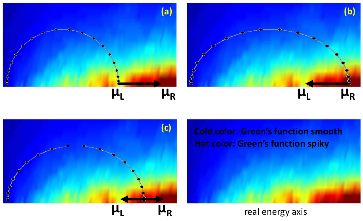
Fig. 8 A typical contour map for calculating the non-equilibrium density matrix using Eq. (4). The complex contour starts from a very large negative energy at least two Rydberg below the band bottom of the device electrodes. The hotter the colour, the more spiky the integrand. In nanodcal, the complex contour can also be divided into more segments each having different number of points for better numerics. For the integration over the bias window, \(\mu_L \rightarrow \mu_R\) , direct computation on the real energy axis is done.(a) The smallSemiCircle; (b) largeSemiCircle; (c) middleSemiCircle.
In the present example, since there is no external bias voltage (see lines 9 and 12 of Au-BDT-Au input), we have \(\mu_L=\mu_R=E_F\) where \(E_F\) is the Fermi level of the gold leads. Therefore the second term of Eq. (4) vanishes and density matrix is obtained entirely by integrating over the semi-circular contour of Fig. 8 (a). Lines 17-18 of Au-BDT-Au input indicate that we shall calculate Eq. (4) using the contour of Fig. 8 (a), and the semi-circular contour is discretized by 40 points.
Lines 20-23 is irreverent for the present case since bias voltage is zero and there is no real energy axis integration. But if the bias were nonzero, these lines would be useful. Line 19 fixes the number of energy points on the horizontal lines of the contour in Fig. 8 (the thick lines with arrow). Line 20 provides a positive imaginary infinitesimal that gets added to the Hamiltonian matrix of the leads for calculating the self-energy of the leads. Line 22 is also a positive imaginary infinitesimal that is added to the Hamiltonian matrix of the scattering region. These infinitesimal parameters provide a small smearing effect to the sharp quantum resonances on the real energy axis. When a system becomes difficult to converge, these smearing parameters can be increased slightly to help. Some times it is possible to start with a rather large smearing parameter (e.g. \(\sim 10^{-3}\)a.u.) and gradually reducing it during the NEGF-DFT iteration to help convergence.
Lines 23-24 specify the convergence criteria, namely we demand the Hamiltonian matrix elements, the density matrix elements and the band energy to converge to \(10^{-5}\)a.u..
The Au/BDT/Au two-probe system involves 110 atoms in the scattering
region. By running NanoDCAL using the scf.input of
Au-BDT-Au input, from the standard output (Matlab command
window) we find that there are total of 1118 valence electrons and 1594
orbitals. The matrix size is therefore \(1594 \times 1594\). The
periodicity along the transverse x,y directions is accounted for by
k-sampling using 30 k-points as shown in Au-BDT-Au input.
This system is best run using a small parallel cluster even though it is
runnable on a good desktop computer, see the corresponding README file
in the /examples/Group10/Au-BDT-Au/ directory.
Green’s functions and the self-energy
In the Eq. (4) above, the density matrix is evaluated by various Green’s functions. Green’s functions are also needed for evaluating the transmission coefficients. As discussed in the Theory section, nanodcal calculates the Green’s functions by direct matrix inversion:
where \(E\) is energy, \(S\) is the overlap matrix, \(H\) the Hamiltonian matrix of the device scattering region, and \(\Sigma\) the self-energy due to the device leads. The superscripts \(R,A\) indicates the retarded and advanced quantities, respectively, and \(\bf{ G}^{A}\ =\ \left(\bf{ G}^{R}\right)^{\dagger}\).
In the last section, when the two probe calculation of Au/BDT/Au device was carried out, NanoDCAL has evaluated Eq. (5) in each step of the self-consistent NEGF-DFT iteration where the self-energy \(\Sigma^{R}=\Sigma^R (E)\) is needed. In NanoDCAL, the computation of \(\Sigma^R\) is done by a plug-in calculator having two methods - NanoDCAL may switch during the run to get best convergence. Since this computation is by a plug-in calculator, it means users can actually calculate \(\Sigma\) using methods of their own - instead of using the methods of NanoDCAL. See Input reference section for more details.
The principle of calculating \(\Sigma\) for device leads is shown in Fig. 9. As already mentioned above, in a two probe calculation the infinite device system becomes the scattering region plus \(\Sigma\). In the Green’s function theory, what has been done is to integrate out the degrees of freedom in the semi-infinite lead regions whose effects to the scattering region are provided by \(\Sigma\). Therefore, once \(\Sigma\) is obtained the actual DFT computation box only includes the scattering - although now the potential in the Hamiltonian is added by a term \(\Sigma\), as shown in Eq. (5).
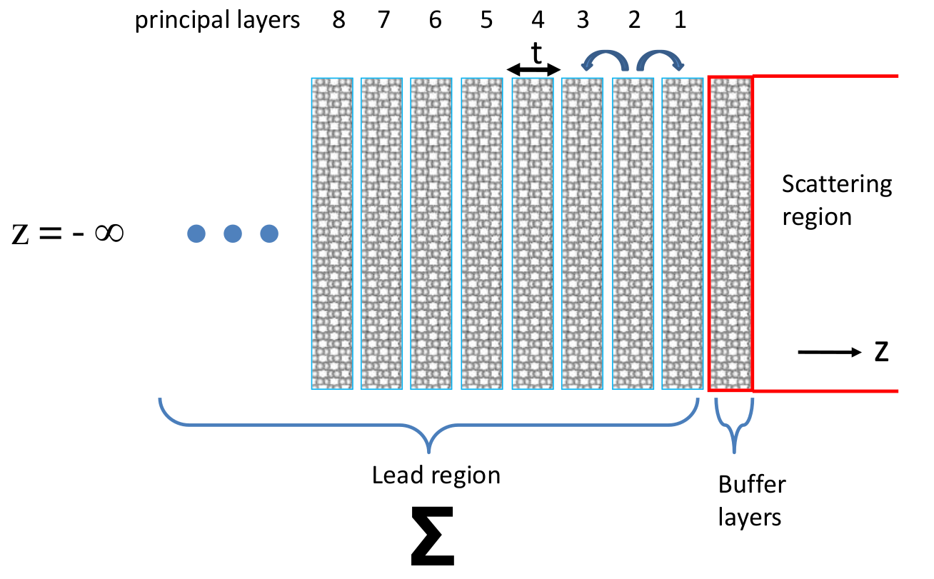
Fig. 9 Side view of a semi-infinite left lead of a device that extends to \(z = −\infty\). The semi- infinite lead geometry is divided into a buffer region containing a few atomic layers, plus the lead region. The buffer region is made of the same lead atoms and structure, but it is part of the device scattering region. In Green’s function theory, the lead region contributes a self-energy \(\Sigma\) to the Hamiltonian of the scattering region.
The calculation procedure of \(\Sigma\) is depicted schematically in Fig. 9 where the semi-infinite lead region is divided into infinite number of identical principle layers (PL) each having width \(t\). In NanoDCAL, \(t\) is required to be thick enough so that a PL has direct orbital overlap only with its nearest neighbor PLs. Furthermore, the box containing the buffer region should have enough atomic layers so that atomic orbitals in PL-1 does not extend to the right of the surface. This is also necessary to screen out any interaction between the atoms inside the scattering region to those inside the leads [TGW01].
A PL in the leads has a finite number of atoms. If the leads are periodic in the transverse x,y directions, a k-sampling technique is applied to the PL along those directions. If the leads have a finite cross section, large enough vacuum regions should be applied to surround the quasi-1d leads. \(\Sigma\) can be calculated in principle by iterating the Dyson equation starting from the first PL by successive addition of the second, third and further PLs until numerical convergence. Practically this is a very slow process. The plug-in calculators of NanoDCAL uses other methods as described in the Theory section.
Calculating transmission coefficient
After the self-consistent NEGF-DFT is completed, we can calculate
physical quantities. In the /examples/Group10/Au-BDT-Au/system/
directory of NanoDCAL, there is an input file transmission.input
which has the following lines:
system.object=‘NanodcalObject.mat’
calculation.name = transmission
calculation.transmission.energyPoints = [-10.00:0.01:10.00]
calculation.transmission.method = GreenFunction
calculation.transmission.leadPairs = [1,2]
calculation.transmission.etaSigma = 1e-5
calculation.transmission.etaGF = 0.0
Line-3 tells NanoDCAL to calculate transmission coefficient for the energy range -10eV to +10eV in steps of 0.01eV. The units of energy is eV - the default, because we did not specify other units in the above. Line-4 tells NanoDCAL to calculate transmission using the Green’s function method. Line-5 says that transport is from lead 1 to lead 2, this line is actually unnecessary because we only have two leads. But for multi-probe systems, one may wish to tell NanoDCAL which pair of leads should be considered otherwise all pairs will be calculated automatically. Lines 6 and 7 sets up two infinitesimal smearing parameters, one for computing self-energy \(\Sigma\) and other for computing the retarded Green’s function. There are many other things one can do to extract quantum transport properties, refer to the Input reference. For example, by replacing the ‘transmission’ in line-2 with ‘conductance’, we can obtain conductance of the system.
Calculating scattering states
Scattering states are eigen-states of the open device structure that
traverse the device from \(z=-\infty\) to \(z=+\infty\). It is
very useful to gain insight to transport problems. In the
/examples/Group10/Au-BDT-Au/system/ directory, there is an input file
scattering.input which has only three lines:
system.object=‘NanodcalObject.mat’
calculation.name = ss
calculation.scatteringStates.plot = true
This calculation will be done with default parameters. In particular, by default the scattering states at the chemical potential of the left and right leads will be obtained. For this particular problem, these chemical potentials are the same. If you wish to calculate scattering states at a number of energies, the following keyWord allows you to specify them:
calculation.scatteringStates.energyPoints = [-1:0.2:1]
Calculating DOS
Similar to the crystal calculation, in two probe calculation we may wish
to obtain the density of states of the device scattering region. In the
/examples/Group10/Au-BDT-Au/system/ directory, there is an input file
dos.input which has the following lines:
system.object=‘NanodcalObject.mat’
calculation.name = dos
calculation.densityOfStates.energyPoints = [-10.00:0.01:10.00]
calculation.densityOfStates.method = GreenFunction
calculation.densityOfStates.eta = 1e-5
Here, lines 3 and 4 tell NanoDCAL to obtain DOS in energy range from -10eV to +10eV in steps of 0.01eV, by Green’s function method. Line 5 is an infinitesimal smearing parameter in the DOS calculations.
Calculating I-V curve
In the /examples directory, there are several I-V curve calculation
examples. For a quick run (on a laptop), let’s go to the
/Group4_C_TwoProbe subdirectory which calculates the I-V curve for a
simple carbon chain. The current for each bias voltage is calculated
from transmission coefficient (see Theory section),
where \(f_{\alpha}(\epsilon)\) is the distribution function of the electrons in lead \(\alpha\); the factor of 2 comes from the spin degeneracy; and \(V_b\) is the bias voltage. From this equation, it is clear that one has to obtain transmission coefficient \(T_{\alpha\beta}(\epsilon, V_b)\) versus bias \(V_b\) before calculating the I-V curves. There are two methods of getting an I-V curve.
Method 1 - calculate each \(V_b\) separately
Since calculating the self-consistent Hamiltonian of the device involves substantial work, we strongly recommend that one obtains them at the desired bias \(V_b\) values separately and then calculate electric current afterward. This is why there are several subdirectories in /Group4_C_TwoProbe/ which are for calculating the system at \(V_b\) between \(0\) to \(1\) volt.
Thus, to obtain an I-V curve, one first completes the lead calculation
in the /Group4_C_TwoProbe/lead/ directory. After you have done that,
please go to each subdirectory named /systemXV where X is a number
which, for convenience, indicates the bias voltage value. You can find
several input files and please run scf.input. After you have run all
the scf.input in these /systemXV directories, you have obtained the
self-consistent device Hamiltonian at the given bias \(V_b\).
While these are routine calculations, in the /system1V/ case, please
open the scf.input and you will notice that we have added transmission
coefficient and conductance as our SCF convergence criterion. Because
these are the physical quantities we are interested in, monitoring them
during the SCF run can be quite useful.
Go to the /Group4_C_TwoProbe subdirectory, there is an input file
ivcurve.input which has the following lines:
% The input file for the i-v curce calculation.
% The files NanodcalObject.mat in the directories system0V and system1V are
% needed for the calculation.
% type "nanodcal -parameter ? calculation.IVCurve" for a complete list
% of input parameters which are used for the i-v curve calculation.
% no default value for the calculation name; must be given.
calculation.name = ’ivc’
% type "nanodcal -parameter ? calculation.name" for a complete list of
% calculation names.
% some input parameters for the calculation.
calculation.IVCurve.systemObjectStatus = ’AllCalculated’
calculation.IVCurve.systemObjectFiles = ...
{’./system0V/NanodcalObject.mat’, ...
’./system1V/NanodcalObject.mat’}
calculation.IVCurve.plot = true
% type "nanodcal -parameter ? calculation.IVCurve" for a complete list
% of input parameters which are used for the i-v curve calculation.
Here, line-1 tells NanoDCAL to calculate an I-V curve using the object files specified in line-3. Line-2 tells NanoDCAL the calculation status of the self-consistent field of the system. ‘AllCalculated’ means the Hamiltonian calculation has already been completed under all the bias voltages. Finally line-4 plots an I-V curve such that a figure is plotted after the ivc run. There are two currents in the figure, \(I_1\) and \(I_2\), measured in the first lead or 2nd lead, respectively. Clearly, \(I_1=-I_2\) for any two-probe steady state situation.
Method 2 - calculate all \(V_b\) in one shot
While the method in the last subsection is what we recommend, one can
also compute the entire I-V curve in one shot without preparing the SCF
for each bias \(V_b\) separately. The reason we do not recommend
this method is because for most practical research problems, the
computation is dominated by individual \(V_b\) calculation of the
SCF. Nevertheless, you can do a one-shot calculation that ends up to the
I-V curve. In the ivcurve1.input file, the essential lines are:
calculation.name = ivc
calculation.IVCurve.systemObjectStatus = AllToBeCalculated
calculation.IVCurve.leadsVoltages = {0, 0:0.2:1}
calculation.IVCurve.plot = true
Line-2 tells NanoDCAL that everything (except the leads) needs to be calculated, e.g. in one shot. Line-3 tells NanoDCAL that \(V_b\) on the first lead (left) is zero, and on the right lead to be values of \(0\)V to \(+1\)V in steps of 0.2V. Note the resulting I-V curve is the same as that obtained in the last subsection.
Resume an interrupted calculation
Some times a self-consistent calculation is interrupted before completion due to hardware stoppage, or by human intervene in order to change some calculation parameters. One can resume the interrupted calculation from the saved temporary files. In the directory of your interrupted project, type the following to resume a calculation using exactly the same control parameters as before:
nanodcal -resume
If you made changes to parameters in the scf.input file, type:
nanodcal -resume scf.input
Convergence issues
Usually, a two probe calculation can be substantially more difficult to
converge than molecule or crystal calculations. Of course, an erroneous
setting of parameters can cause the problem. If all are set up
correctly, it may still take a large number of steps - even beyond our
patience, to converge. Very roughly - and depending on the system, a two
probe calculation can take several times or even more iteration steps to
converge than a crystal calculation of a similar sized system.
NanoDCAL sets a default SCF iteration steps at 50 which may not be
enough and you can increase this number by adding a line in the
scf.input file, e.g.:
calculation.SCF.maximumSteps = 200
There are several possible reasons for a slow convergence behavior. One is due to the existence of many singularities near the real energy axis that makes a accurate calculation of the density matrix difficult to achieve. Namely, for many cases the integrand in Eq. (4) have sharp resonances when energy \(E\) is on or near the real axis and Fig. 8, obtained from a real calculation in a two probe carbon nanostructure, clearly shows where the resonances lie. One may improve the convergence by increasing the number of energy points and the number of k-points for each \(E\), on the part of the contour close to the real axis. One may also try different contours as shown in Fig. 8. In the section entitled “Energy contour parameters” of the Input reference section, there are other parameters one may experiment. For instance by increasing various smearing parameters one usually can help smoothing the sharp resonances and, after the convergence gets better one can reduce these smearing gradually to very small values (\(\sim 10^{-6}\)). One may include an electron temperature that also smears singularities to some extent (also add Fermi poles on the imaginary energy axis) of the contour integration in Fig. 8 .
Another possibility is to switch to a different mixer, or change the
mixed quantity, or a combination of them. NanoDCAL has several
commonly used mixers as described in the Input reference section. Users
can also supply their own mixers. Please read
section Calculating the scattering region above and the Input reference section for more
discussions on the mixers. To switch a mixer, just stop the run, make
change in the scf.input, and resume the run (see
subsection Resume an interrupted calculation above.
For open systems, experience suggests that the initial condition of a calculation becomes much more important than that of crystal/molecule calculation. The default, namely the neutral atom density (see Theory section), is quite good for crystal and molecule calculations. For open systems it is less satisfactory. Therefore a better starting point may be one from a previous calculation. For instance if one wants to obtain results at a bias voltage of 0.2V, perhaps the initial density should be that obtained at bias of zero volt, etc. To load in an initial density or Hamiltonian is very easy in nanodcal, by adding the following line to the scf.input:
calculation.SCF.donatorObject = NanodcalObject.mat
the new calculation will start from the initial data contained in the
object file NanodcalObject.mat.
For really difficult two probe situations, one may consider building a periodic crystal using the central region of the device as the supercell, converge it and save the density. This is usually not difficult to achieve because it is much easier to converge crystal calculations. One then load in the save density (or other quantities) as the initial condition to start the two probe device simulation. We have used such tricks to converge many very difficult systems.
We emphasize that NEGF formalism for quantum transport involves open systems where the Hamiltonian matrix of the device scattering region is non-Hermitian due to the complex self-energies \(\Sigma^{R,A}\). This means there is no minimization principle to follow. Furthermore, in the NEGF-DFT analysis, the Fermi level of the entire device is fixed by the device leads thus cannot be adjusted during the SCF iteration cycle. Together with the singularities in the Green’s functions on the real energy axis, they contribute to the difficulty of numerical convergence.
Summary
This Section briefly summarizes the most important function of NanoDCAL, namely quantum transport analysis of open device structures. Referring to the Theory section and the Input Reference manuals, you can find that nanodcal has many powerful functionalities for nonequilibrium and nonlinear quantum transport capabilities.
A two probe calculation can be substantially more difficult to converge than molecule or crystal calculations as discussed in Section 1.8 <#sec-convergence above. However, practice and experience usually help users to develop intuitive understanding of the SCF process in open structures.
Finally, in the /example directory, we also prepared several two probe
transport examples that require parallel computation. These substantial
examples are grouped in the subdirectory /example/Group10/, all of them
are from real research problems published in the literature. These
examples have been run on a (not too old) Linux parallel cluster of 8
processors (one used 32 processors). Further information can be found in
the README files associated with these examples.
Taylor, J., Guo, H., & Wang, J. (2001). Ab initio modeling of quantum transport properties of molecular electronic devices. Physical Review B, 63(24), 245407.