Silicon Transistor tutorial
Requirements
Software components
nanotools
NanoDCAL+
Structure file
slab.xyz
Pseudopotentials
H_AtomicData.mat
Si_AtomicData.mat
Copy the mat files from the pseudo database to the current working directory and export NANODCALPLUS_PSEUDO=$PWD.
References
Briefing
In this tutorial, we demonstrate simulating the on-off transport property of a npn silicon based junction.
We apply a source-drain bias over the junction and compute the charge current for a series
of gate voltages.
The atomic structure of the transport junction is shown in the following figure
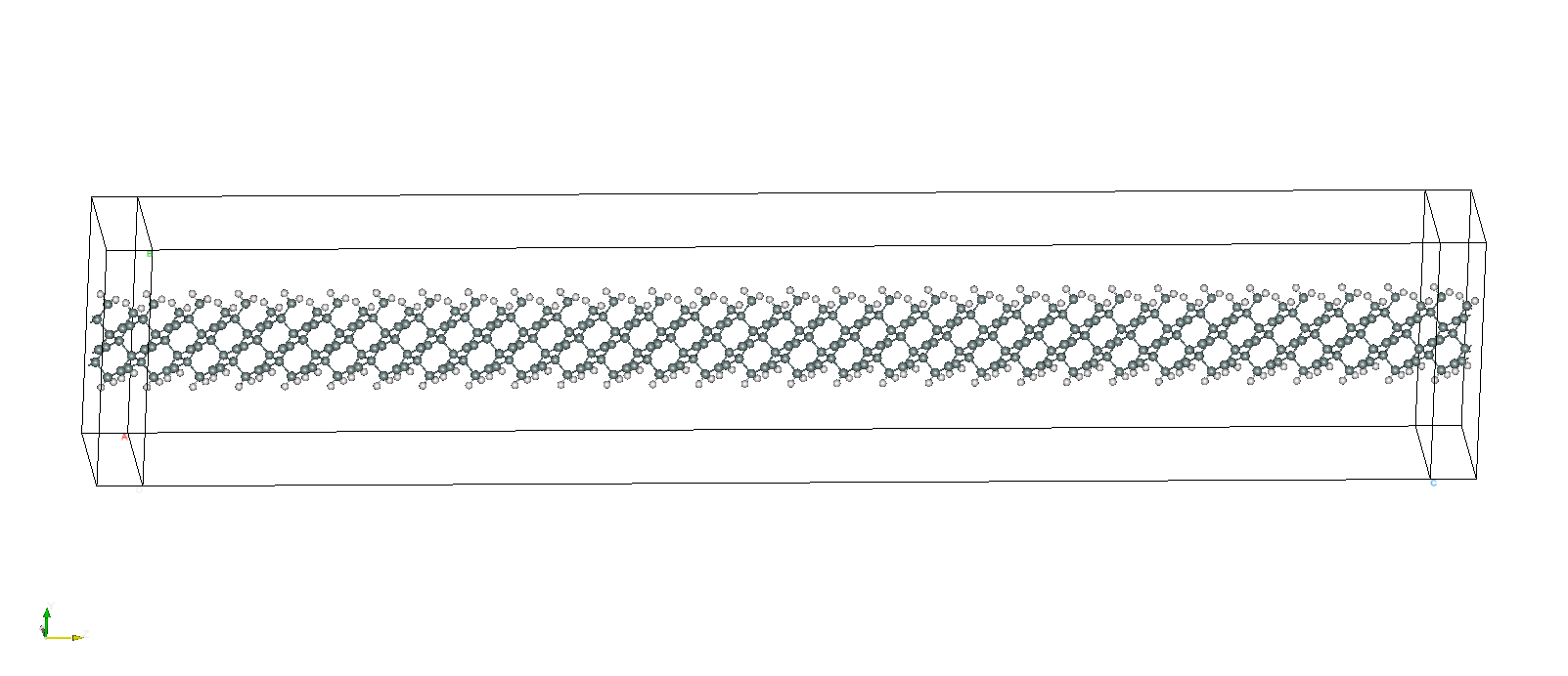 The z-direction is chosen as the transport direction.
The whole system has a slab geometry, periodic in the x-direction and passivated by hydrogen atoms in the y-direction. Above and below the passivated surfaces are dielectric media as indicated in the following figure
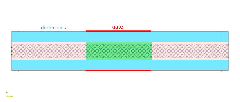
P-doped silicon atoms are highlighted in green, and the rest are n-doped. We introduce two gates at the top and bottom of the simulation box, so as to tune the electrostatic potential within the transport channel; without gates, the junction is naturally in the off-state.
Full script
The following script is used to compute the charge current under a gate-source voltage of 0.5 V and a
drain-source bias of 0.2 V. The result, a single number with proper unit, is printed out on the screen at the end.
Besides, standard output files ending with _out.json or _out.h5 are saved in the directory after
the program is finished.
import numpy as np
from nanotools import Atoms, Cell, Current, Pop, Region, System, TotalEnergy, TwoProbe, IV
npc = 40    # number of processors to be used

cell = Cell(avec=[[5.43, 0.0, 0.0], [0.0, 30., 0.0], [0.0 , 0.0 , 5.43]], resolution=0.2)
atoms= Atoms(positions="slab.xyz", doping_ratios="slab.xyz")

pop = Pop(type="fd", contour_type="single", sigma=0.026)
sys = System(cell=cell, atoms=atoms, pop=pop)
sys.kpoint.set_grid([5,1,21])

di1 = Region(fractional_x_range = [0,1], fractional_y_range = [0,0.25], fractional_z_range = [0,1])
di2 = Region(fractional_x_range = [0,1], fractional_y_range = [0.75,1], fractional_z_range = [0,1])
sys.add_dielectric(di1, epsilon=25)
sys.add_dielectric(di2, epsilon=25)
sys.set_open_boundary(['-y','+y'])
left = TotalEnergy(sys)
left.solver.set_mpi_command(f"mpiexec -n 4")
left.solver.restart.densityPath = "left_out.h5"

center = left.copy()
center.supercell(T=np.diag([1,1,30]))
center.system.kpoint.set_grid([5,1,1])
dopp = [.999, .999, .999, 1, 1, .999, .999, .999, .999, 1, 1,
        .999, .999, .999, 1, 1, .999, .999, .999, .999, 1, 1]
dopn = [1.001, 1.001, 1.001, 1, 1, 1.001, 1.001, 1.001, 1.001, 1, 1,
        1.001, 1.001, 1.001, 1, 1, 1.001, 1.001, 1.001, 1.001, 1, 1]
center.system.atoms.set_doping_ratios(dopn*10 + dopp*10 + dopn*10)

g1  = Region(fractional_x_range = [0,1], fractional_y_range = [0,0], fractional_z_range = [.33,.66])
g2  = Region(fractional_x_range = [0,1], fractional_y_range = [1,1], fractional_z_range = [.33,.66])
vgs = +0.5  # gate-source voltage Vg-Vs
wf  = 4.5   # work function
center.system.add_gate(region=g1, work_func=wf, Vgs=vgs)
center.system.add_gate(region=g2, work_func=wf, Vgs=vgs)

center.solver.mix.alpha = 0.1
#center.solver.mix.precond = "kerker"
center.solver.mix.maxit = 120
center.solver.set_mpi_command(f"mpiexec -n {npc}")
center.solver.mix.tol = 1.0e-6
center.solver.mpidist.kptprc = 5  # k-parallelization setting
center.solver.mpidist.zptprc = 4
center.solver.restart.densityPath = "center_out.h5"

vds = 0.2   # drain-source voltage Vd-Vs
dev = TwoProbe(left=left, center=center, transport_axis=2, bias=vds)
dev.solve() # self-consistent calculation

dev.center.system.kpoint.set_grid([25,1,1])  # increase k-points for current computation
cal = Current.from_twoprobe(dev)
I = cal.calc_charge_current()
print(I)
Note that it may take over 60 iterations to reach convergence. In that case, the script needs be run
several times depending on center.solver.mix.maxit parameter. Carefully tune center.solver.mix.alpha if
it helps.
Explanations
Doping level
Just as most semiconductor devices, our silicon-based transistor requires a certain doping level in order to be functionalized. In our code, the doping feature is implemented in an artificial manner (virtual crystal approximation), namely no actual dopants are added into the system. Instead, we specify a doping ratio on each individual atom in the system. A ratio of 1.001 (0.999) means 0.1% of the atom’s valance electrons are to be added (removed).
When we initialize the atoms object as follows
atoms= Atoms(positions="slab.xyz", doping_ratios="slab.xyz")
we set the doping_ratios keyword to be the name of the atomic structure file “slab.xyz”. This means
that the doping ratio on each atom is specified in the structure file. Taking a look into the file,
22
AtomType   X               Y            Z         doping_ratio
Si        2.98168995  12.301750000  0.26668995    1.001
Si        0.26668995  15.016750000  0.26668995    1.001
Si        2.98168995  17.731750000  0.26668995    1.001
H         0.80006984  10.000000000  0.80006984    1
H         5.16331005  20.033523324  0.80006984    1
...
we see that the ratios are listed under the doping_ratio keyword.
It is also possible to set doping ratios for an existing Atoms object, using its set_doping_ratios
method. This method takes in a list of numbers with the same order as the atomic coordinates.
For example, to set the doping ratios in the central region, which consists of ten n-doped unit cells,
followed by 10 p-doped cells, and then followed by another ten n-doped unit cells, we use
dopn = [1.001, 1.001, 1.001, 1, 1, 1.001, 1.001, 1.001, 1.001, 1, 1,
        1.001, 1.001, 1.001, 1, 1, 1.001, 1.001, 1.001, 1.001, 1, 1]
dopp = [.999, .999, .999, 1, 1, .999, .999, .999, .999, 1, 1,
        .999, .999, .999, 1, 1, .999, .999, .999, .999, 1, 1]
center.system.atoms.set_doping_ratios(dopn*10 + dopp*10 + dopn*10)
Remember that the “*” operator for lists means replication and that “+” means concatenation.
Dielectrics and gates
In order to define dielectrics and gates within the system, we first need to create some Region objects
which specify the geometry of the desired object.
di1 = Region(fractional_x_range = [0,1], fractional_y_range = [0,0.25], fractional_z_range = [0,1])
di2 = Region(fractional_x_range = [0,1], fractional_y_range = [0.75,1], fractional_z_range = [0,1])
Region object specifies a rectangular/parallelepiped region in the 3d simulation box. The range in each dimension is specified by
a pair of fractional numbers.
Once a system object is initialized, a dielectric region can be added using the add_dielectric method
with the specified (relative) permittivity, denoted as epsilon, eg
system.add_dielectric(di1, epsilon=25)
system.add_dielectric(di2, epsilon=25)
It is important to specify the proper boundary condition of Poisson equation in accordance with the dielectric configuration. In our case, we put
system.set_open_boundary(['-y','+y'])
which indicates that the Neumann boundary condition is applied to the surfaces normal to y-axis.
Similarly we may create regions for metallic gates
g1  = Region(fractional_x_range = [0,1], fractional_y_range = [0,0], fractional_z_range = [.33,.66])
g2  = Region(fractional_x_range = [0,1], fractional_y_range = [1,1], fractional_z_range = [.33,.66])
and add gates to the system object
system.add_gate(region=g1, work_func=wf, Vgs=vgs)
system.add_gate(region=g2, work_func=wf, Vgs=vgs)
where Vgs denotes the gate-source voltage, and work_func denotes the work-function of the gate material.
Note that, unlike dielectric regions, for gates only 2d geometry is supported. That is why we collapse the
fractional_y_range to [0,0] or [1,1], i.e. only on the surfaces of the simulation box.
The effect of gate is providing a Dirichlet boundary condition for Poisson equation. Only one gate is
allowed on each surface, and Neumann boundary condition is always assumed on the rest of the surface
apart from the gate.
The gate work-function is a parameter we expect to be provided by the user, especially when the user has a specific gate material in mind. Otherwise, we refer to the next section as for estimating a proper work function in case the user simply wants a virtual gate.
Work function of gates
Adding metallic gates to the surface of our simulation box essentially sets a boundary value for the electrostatic potential in the system. However, it is important to take note that this boundary value differs from the gate voltage we apply. In fact, it should be the gate’s work function minus the gate-source voltage. See the diagram below.
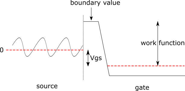
The diagram depicts an imaginary contact between the source and gate materials. As a convention, the chemical potential (Fermi energy, red dashed line) of source is set at zero; that of the gate is somewhat lower as we apply a positive gate-source voltage (remembering electrons have a negative charge). The boundary value provided by the gate is actually the vacuum level of the material, which is equal to its work function minus the gate-source voltage.
Having understood the role of work function, we now demonstrate how to calibrate it in case the user does not have this material parameter at hand or simply wants an effective way to tune the electrostatics via a virtual gate. The goal of this calibration is such that the boundary value stays approximatly the same, whether without the gate at all or with the gate in equilbrium to the source (Vgs=0). To this end, we comment out
#center.system.add_gate(region=g1, work_func=wf, Vgs=vgs)
#center.system.add_gate(region=g2, work_func=wf, Vgs=vgs)
and set the drain-source bias Vds to zero. After the self-consistent calculation is finished,
run the following script to visualize the electrostatic potential on the surface where the gate
is to be placed.
from nanotools import TwoProbe
ecalc = TwoProbe.read(filename="nano_2prb_out.json")
veff = ecalc.smooth_field("potential/effective", axis=2, preslice=lambda a: a[:,-2:-1,:])
fig = ecalc.center.plot_field(veff, axis=2)
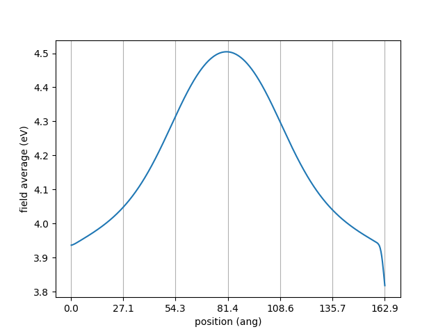
One can see that the electrostatic potential is bumped up in the middle due to the p-n junction effect. The potential in the middle reads 4.5 V. That is what we assign to the gate work function.
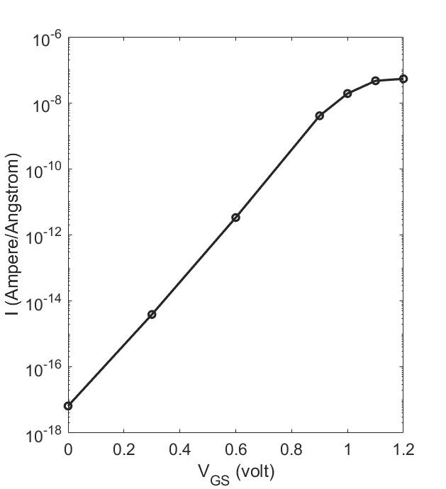
Results
Run the script over and over under a series of gate-source voltages, and read off the current values
printed on screen at the end. The resulting I-Vgs curve looks like
We have implemented an IV calculator to automate this process, i.e. run self-consistent calculations
under a series of voltages, compute the charge currents, collect data and plot the I-V curve. The usage
is as follows
from nanotools import TwoProbe, IV
# see the script at the top ...
dev = TwoProbe(left=left, center=center, transport_axis=2, bias=vds)
calc = IV(reference_calculator=dev,
          k_grid_4_current=[25,1,1],
          varying_elements=center.system.hamiltonian.extpot.gates,
          voltages=[0.0,0.3,0.6,0.9,1.0,1.1,1.2],
          work_func=wf)
calc.solve()
calc.plot(log=True, filename="iv.png")
Or, if there is already an existing nano_2prb_in.json,
from nanotools import TwoProbe, IV
dev = TwoProbe.read("nano_2prb_in.json")
calc = IV(reference_calculator=dev,
          k_grid_4_current=[25,1,1],
          varying_elements=dev.center.system.hamiltonian.extpot.gates,
          voltages=[0.0,0.3,0.6,0.9,1.0,1.1,1.2],
          work_func=4.5)
calc.solve()
calc.plot(log=True, filename="iv.png")
The IV calculator is initialized with the reference TwoProbe calculator, a varying_elements
list containing the gate objects whose voltages we wish to vary (in our case we wish to vary both gates
simultaneously), a range of voltages in voltages, and the work-function of the gates.
calc.solve() then carries out self-consistent calculations and computes the corresponding
currents, which are stored in calc.currents attribute. Finally, calc.plot(log=True) plots the I-V curve in log-scale.
Note that, during the process, there is no guarantee that the self-consistent calculations are well
converged: they may stop simply because the number of iterations has hit mixer.maxit. In this case,
the user may want to run calc.solve() several times until convergence is reached under each voltage.
Alternatively, the user can enter each of the spawned directories, whose name ends with the corresponding
voltage value, and manually launch computations from therein.
From the above figure, we see that the current gets switched on as the gate voltage goes more positive, as expected for a npn junction. To have a closer look, we plot the effective potential using the following script
ecalc = TwoProbe.read(filename="nano_2prb_out.json")
veff = ecalc.smooth_field("potential/effective", axis=2, preslice=lambda a: a[:,60:90,:])
fig = ecalc.center.plot_field(veff, axis=2, filename="potential.png")
on the results obtained under Vgs=0 V and 1 V respectively. The figure is shown below
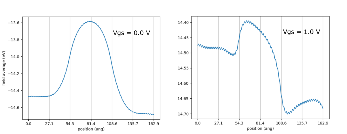
As one can see, the potential barrier for electrons gets significantly lowered at Vgs=1 V, hence allowing for more charge flow.