2. Workflow for QTCAD® simulations
In this section, we explain the basic workflow for TCAD simulations with the QTCAD device simulator. We first summarize the main steps of QTCAD simulations. We then explain the two main techniques for geometry definition that are currently supported by QTCAD: defining a planar geometry from a device layout using devicegen, or defining arbitrary 1D, 2D, or 3D geometries with Gmsh.
2.1. QTCAD simulations
Any QTCAD simulation may be divided in the following three steps.
Geometry specification and meshing
Physical problem specification and solution
Postprocessing
In this section, we will first cover all three steps of a QTCAD simulation by considering two main workflows: the Gmsh workflow and the devicegen workflow. We will do this by considering two examples: a nanowire device and a gated quantum dot.
2.1.1. Example 1: Nanowire device
As a first example in this section, we consider the nanowire device illustrated below.
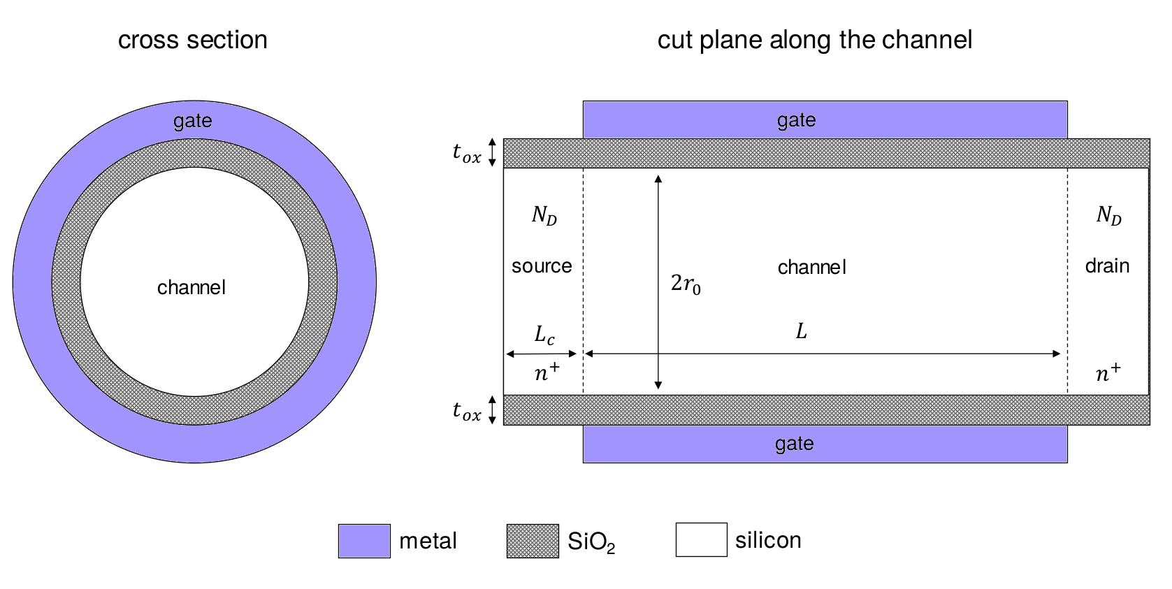
Fig. 2.1.1 Structure of the nanowire under consideration (image courtesy of Qing Shi from McGill University)
The nanowire is a structure modeled by two concentric cylinders whose common rotational symmetry axis is aligned with \(z\). The inner cylinder is filled with silicon, while the shell formed by the region between the inner and outer cylinders is filled with silicon dioxide. The two ends of the silicon cylinder (the source and drain) are p-doped while the central silicon region (the channel) is undoped. A metallic gate wraps around the channel; in addition, the external faces of the source and drain regions are kept at equilibrium with Ohmic contacts.
2.1.2. Example 2: Gated quantum dot
As a second example in this section, we consider the gated quantum dot device illustrated below.
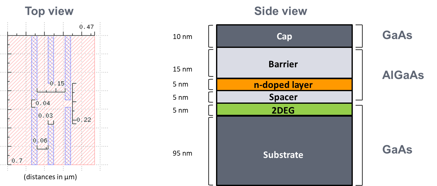
Fig. 2.1.2 Structure of the gated quantum dot under consideration
The top view (\(x\)–\(y\) plane) shows a layout of the 2D gate geometry for this device. The blue rectangles represent metallic gates used to define the confinement potential within the \(x\)–\(y\) plane. The red rectangle represents the extent of the simulation domain.
The side view represents the heterostructure stack along the growth axis (\(z\)) of the chip wafer. As the conduction band edge of AlGaAs is higher in energy than that of GaAs, the AlGaAs layer acts as a potential barrier that prevents conduction between the substrate and the top gates. In addition, doping within the AlGaAs layer leads to band bending that causes a triangular confinement potential well to form right at the interface between the GaAs substrate and AlGaAs, in the region labeled as “2DEG” in the above figure.
The combination of confinement along the \(z\) direction provided by the heterostructure with confinement within the \(x\)–\(y\) plane produced by the top gates is expected to lead to the existence of bound states in the 2DEG region and at the center of the \(x\)–\(y\) plane (between the top gates). These bound states may then be used to implement a quantum dot.
2.2. Geometry specification and meshing
In this subsection, we explain how the device geometry may be specified using either the Gmsh workflow (example 1) or the devicegen workflow (example 2).
2.2.1. Regions and boundaries
Before jumping into geometry specification for each workflow, it is important to discuss general features of device geometry.
Any device may be divided into regions and boundaries, as illustrated below.
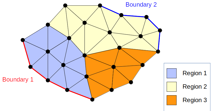
Fig. 2.2.1 Schematic of an arbitrary device: its mesh, its regions, and its boundaries
In the above figure, circles represent finite-element nodes, while straight lines represent element edges.
Regions are subsets of the simulation domain labeled with an integer or string. Regions may be associated to a material or set of physical properties (e.g. doping density). In the nanowire example (example 1), these regions are the source, drain and channel, as well as the oxide that surrounds each of these. Depending on dimensionality, regions may be either volumes (3D simulations), surfaces (2D simulations), or lines (1D simulations).
Likewise, boundaries are surfaces (3D simulations), curves (2D simulations) or points (1D simulations) labeled by an integer or string. These geometric entities are used to specify boundary conditions for differential equations solved in QTCAD (e.g. Poisson’s equation).
2.2.2. Arbitrary geometry definition with Gmsh
Using Gmsh, it is possible to define arbitrary 1D, 2D, and 3D device geometries and mesh them. In addition, Gmsh allows users to label regions and boundaries through physical volumes, surfaces, curves, or points. In the nanowire example (example 1), such labeling is illustrated below.
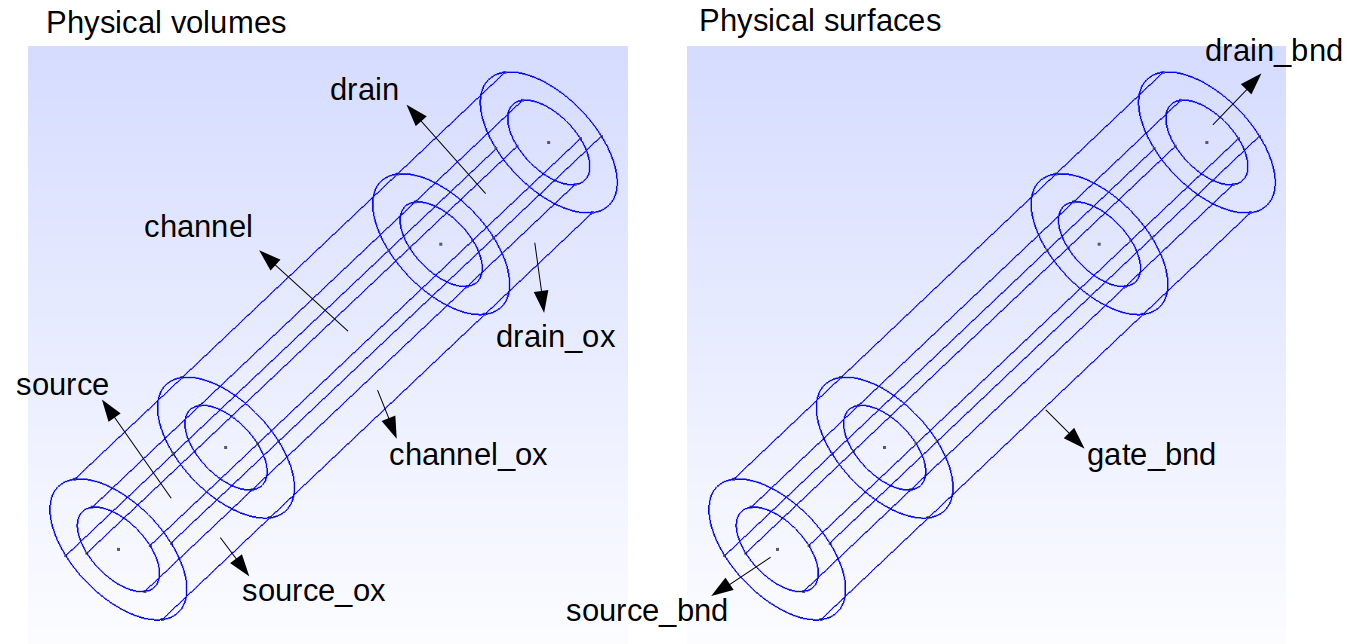
Fig. 2.2.2 Gmsh physical volume and surface labels for a nanowire
To learn how to use Gmsh for arbitrary geometry definition and meshing, we recommend reading the official Gmsh tutorials. There are also some excellent Gmsh tutorials covering the basic concepts available on YouTube, such as this one.
Gmsh is a scripting language at its core; however, it also comes with a
basic Graphical User Interface (GUI) that enables straightforward visualization
and geometry definition. Each GUI action has an equivalent script line which is
stored in the .geo file.
The .geo file that enables to generate the nanowire geometry of example 1
may be found in qtcad/examples/tutorials/meshes/nanowire.geo.
This file contains instructions to create the bottom drain and oxide surfaces
and extrude them along the \(z\) direction to form a semiconductor nanowire
surrounded by oxide. We will assume
that the user has read the Gmsh documentation to be able to understand
this simple script. It is also straightforward to produce a similar script by
drawing the geometry using the Gmsh GUI.
The most important pieces of code for the purpose of integrating with QTCAD are the definitions of the physical volumes and surfaces for the device. This is done at lines 66-68
Physical Surface("drain_bnd") = {1};
Physical Volume("drain") = {volume_drain};
Physical Volume("drain_ox") = {volume_drain_ox};
lines 86-89:
Physical Volume("channel") = {volume_channel};
Physical Surface("gate_bnd") = {sides_channel_ox[0],
    sides_channel_ox[1], sides_channel_ox[2], sides_channel_ox[3]};
Physical Volume("channel_ox") = {volume_channel_ox};
and lines 107-109
Physical Surface("source_bnd") = {top_source};
Physical Volume("source") = {volume_source};
Physical Volume("source_ox") = {volume_source_ox};
of the nanowire.geo file. Importantly, these lines specify labels
(e.g. "channel") for the device’s volumes and surfaces, which can be used
by QTCAD functions to assign various physical properties (e.g. material
composition, external voltages) to them.
Another key step is to generate and save the mesh. This is done in lines
111-114 of the nanowire.geo file:
Mesh 1;
Mesh 2;
Mesh 3;
Save "nanowire.msh";
Note
QTCAD currently supports .msh2 and .msh4 (equivalent to .msh) formats.
To visualize the mesh produced by the nanowire.geo file and save it in .msh
format, from the root of the QTCAD directory, type:
gmsh examples/tutorials/meshes/nanowire.geo
This will save the mesh file (nanowire.msh) in the same directory as the
.geo file.
2.2.3. Planar geometry definition with devicegen
While Gmsh is very powerful and flexible, it is often time-consuming to define device geometry explicitly by manually defining the structure in the GUI or by writing a script.
In particular, gated quantum dots often display complicated 2D gate patterns used to confine individual electrons or holes. For example, Fig. 2.1.2 shows six individual top gates, a number that increases quickly as the number of quantum dots rises. Manually defining those gates in combination with the heterostructure stack is often tedious.
To define planar device geometries, it is often more convenient to use
devicegen.
The devicegen package uses Gmsh as a dependency to produce specific
geometries more easily.
Indeed, devicegen can load layouts from text GDS files to define the
gate pattern. The geometry along the growth direction (heterostructure
stack) is then defined through devicegen’s simple Python API.
The resulting structure can finally be exported in .msh format.
For more information on how to use devicegen, it is recommended to go through the devicegen tutorial, which explains in detail how to produce the geometry illustrated in Fig. 2.1.2.
In addition, it is important to note that devicegen is currently released as open-source code within the GPL license. Indeed, we invite motivated users with specific design rules in mind that are not directly coded in devicegen to propose modifications to the package through its public GitHub repository.
Just like Gmsh, devicegen enables to label regions and boundaries and
save them with the mesh in a .msh file.
This information will be used next in the definition of a physical model for
the system to simulate.
2.3. Physical problem specification and solution
Once the mesh is generated and saved in .msh format, it is loaded into
QTCAD using its Python API. A device object (materials, doping densities,
boundary conditions, etc.) may then be specified, and relevant solvers may be
instantiated and launched.
There are several solvers available in QTCAD, and the best way to learn how to use them is to go through the tutorials for spin qubits or superconducting circuits. Nevertheless, all QTCAD simulations share a common structure, which we illustrate here in the context of examples 1 and 2 by showing the codes for very basic QTCAD simulations. In these simulations, the non-linear Poisson equation is solved, giving the electric potential configuration for a certain set of gate potentials in the presence of classical carrier reservoirs.
Even though this is a classical calculation, it plays an important role in QTCAD because the resulting electric potential may be used to calculate the confinement potential of electrons or holes in the device. This potential may then be used to define effective Schrödinger equations for electrons or holes in the nanostructure, calculate bound states, write down a many-body Hamiltonian, and diagonalize it to find the chemical potentials of quantum-dot systems.
In both examples, we give minimal pieces of code to run this simple calculation. You can find more details, including more advanced functionalities, in the tutorials for spin qubits or superconducting circuits. In addition, each of the API commands used below is described in more details (including detailed descriptions of all arguments) in the APIreference.
2.3.1. Example 1: nanowire
In this example, we run the simple simulation described above for the mesh
produced by examples/tutorials/meshes/nanowire.geo. Here, we concentrate on
the structure of the script, a more detailed version of this first example
may be found in Poisson and Schrödinger simulation of a nanowire quantum dot.
The relevant modules of the QTCAD API are first loaded with
from qtcad.device import constants as ct
from qtcad.device.mesh3d import Mesh
from qtcad.device import materials as mt
from qtcad.device import Device
from qtcad.device.poisson import Solver
We also import pathlib and define the path to the mesh file we wish to
import, which we assume to be stored in the meshes directory lying next to
the Python script we are running.
import pathlib

script_dir = pathlib.Path(__file__).parent.resolve()
path_mesh = script_dir / "meshes/" / "nanowire.msh"
Next, we load the mesh, and instantiate a Device object over this mesh.
scaling = 1e-9
mesh = Mesh(scaling, str(path_mesh))
d = Device(mesh)
The first argument of the Mesh constructor specifies length units. Since
QTCAD uses SI base units, using scaling=1e-9 means that length
units in the mesh file are taken to be nanometers.
Once the device is instantiated, we first define regions, and then boundaries (see Boundary Conditions). It is important to define regions before the boundaries, since the mathematical formulas that determine the electric potential at boundaries depend on parameters (e.g. doping density) that are specified when defining regions.
d.new_region('channel_ox',mt.SiO2)
d.new_region('source_ox',mt.SiO2)
d.new_region('drain_ox',mt.SiO2)
d.new_region('channel', mt.Si)
d.new_region('source', mt.Si, pdoping=5e20*1e6, ndoping=0)
d.new_region('drain', mt.Si, pdoping=5e20*1e6, ndoping=0)

d.new_ohmic_bnd('source_bnd')
d.new_ohmic_bnd('drain_bnd')

Vgs = 0.5
Ew = mt.Si.chi + mt.Si.Eg/2
d.new_gate_bnd('gate_bnd',Vgs,Ew)
Above, we have specified that the source and drain are p-doped silicon with doping density \(5\times 10^{20} \textrm{ cm}^{-3}\) (we multiply by \(10^6\) to convert to \(\textrm{m}^{-3}\)), that the channel is intrinsic silicon, and that the source, channel and drain are surrounded by silicon dioxide. We have also specified that the source and drain boundaries are Ohmic, and that the gate that wraps around the channel has an applied potential of \(0.5\textrm{ V}`\) and a workfunction at midgap.
Once the regions and boundaries of the device are configured, we are ready to instantiate the non-linear Poisson solver and run it. This is done with:
s = Solver(d)
s.solve()
The resulting electric potential is stored in the device attribute phi.
2.3.2. Example 2: Gated quantum dot
In this second example, we consider a gated quantum dot simulation performed
using the .msh file produced by the
devicegen tutorial.
As in example 1, we first import relevant modules.
from qtcad.device import constants as ct
from qtcad.device import materials as mt
from qtcad.device.mesh3d import Mesh
from qtcad.device import Device
from qtcad.device.poisson import Solver, SolverParams

import pathlib
We then import the mesh saved in the gated_dot.msh file produced in the
devicegen tutorial,
which we assume to be stored in a meshes directory alongside the Python
script that we are running. We also instantiate a device over this mesh.
script_dir = pathlib.Path(__file__).parent.resolve()
path_mesh = str(script_dir/'meshes'/'gated_dot.msh')

scaling = 1e-6
mesh = Mesh(scaling,path_mesh)
d = Device(mesh)
d.set_temperature(0.1)
Here, we have set the device temperature to be \(0.1\textrm{ K}\) (we assume temperature to be uniform).
We then set the materials for each region labeled in the tutorial.
d.new_region("cap", mt.GaAs)
d.new_region("barrier", mt.AlGaAs)
d.new_region("dopant_layer", mt.AlGaAs, ndoping=3e18*1e6)
d.new_region("spacer_layer", mt.AlGaAs)
d.new_region("spacer_dot", mt.AlGaAs)
d.new_region("two_deg", mt.GaAs)
d.new_region("two_deg_dot", mt.GaAs)
d.new_region("substrate", mt.GaAs)
d.new_region("substrate_dot", mt.GaAs)
Once the materials are set, it is important to align the bands across hetero-interfaces. By default, QTCAD uses Anderson’s rule to align bands. However, Anderson’s rule is known to be only qualitatively correct. For GaAs/AlGaAs hetero-interfaces, we have calculated more accurate band alignment parameters using our atomistic simulation code RECU (see Band alignment from atomistic simulations). We activate this band alignment model with:
d.align_bands(mt.GaAs)
As before, we continue by setting the boundary conditions for the system. Here, we use an Ohmic boundary condition for the surface at the very bottom of the simulation domain (bottom of the substrate in Fig. 2.1.2). We also use Schottky boundaries for all the top gates, which take as arguments the applied potential and the Schottky barrier height.
d.new_ohmic_bnd("back_gate")

barrier = 0.834*ct.e
d.new_schottky_bnd("top_gate_1", -0.5, barrier)
d.new_schottky_bnd("top_gate_2", -0.5, barrier)
d.new_schottky_bnd("top_gate_3", -0.5, barrier)
d.new_schottky_bnd("bottom_gate_1", -0.5, barrier)
d.new_schottky_bnd("bottom_gate_2", -0.5, barrier)
d.new_schottky_bnd("bottom_gate_3", -0.5, barrier)
Next, we instantiate a Poisson solver, and run it.
solver_params = SolverParams({"tol": 1e-3, "maxiter": 100})
solver = Solver(d, solver_params=solver_params)
solver.solve()
Here, we have defined a SolverParams object which is used to set
parameters of the Poisson solvers. We have set the tolerance of the
self-consistent solver (tol argument) to \(10^{-3}\textrm{ V}\) and the
maximum number of iterations (maxiter argument) to \(100\). This means
that we require the maximum difference between the electric potentials
of two successive iterations to be less than \(1\textrm{ mV}\) for the
self-consistent loop to stop, unless the maximum number of iterations has been
reached, in which case the simulation is forced to stop with a warning message.
Note that each module defining a Solver class also contains an associate
SolverParams class; here we use the
SolverParams class of the
poisson module, for obvious reasons.
2.4. Postprocessing
Once a simulation is completed, it is important to be able to visualize the results and perform some qualitative or quantitative analysis.
There are two main ways to do this in QTCAD:
Using the
analysismodule of QTCAD.Using ParaView.
In the first case (analysis), we produce plots, linecuts, slices, and
other visualization tools directly within a QTCAD script. The analysis
module leverages Matplotlib for 2D plotting, and PyVista for 3D
plotting.
In the second case (ParaView), we save the results of a simulation in
a .vtu file which may then be loaded into
ParaView, an open-source,
multi-platform 3D data analysis and visualization application.
ParaView is very powerful and much more complete than the analysis
module; therefore, we recommend using it for any serious data analysis.
However, for simple plots and sanity checks, it is often convenient to
use the analysis module to produce plots without leaving the QTCAD API.
This is done in most of the tutorials.
Here, we show quickly how to handle both approaches in example 1 (nanowire). The same commands would equally work in example 2.
2.4.1. Postprocessing with the analysis module
We first import the analysis module with
from qtcad.device import analysis
We then produce a plot of the electric potential on a linecut along the \(z\) axis (symmetry axis of the cylinder).
analysis.plot_linecut(mesh,d.phi,(0,0,0),(0,0,20e-9),
   title='Electric potential (V)')
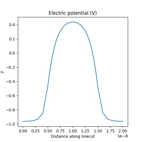
Fig. 2.4.1 Potential along the symmetry axis of the nanowire.
We may also produce a band diagram along the same linecut.
analysis.plot_bands(d, (0,0,0), (0,0,20e-9))
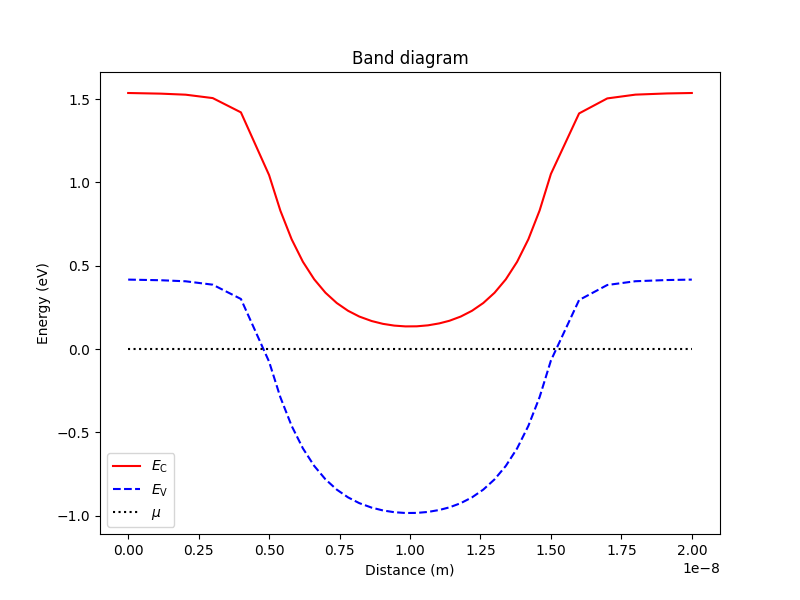
Fig. 2.4.2 Band diagram along the symmetry axis of the nanowire.
Finally, it is also possible to visualize results in 3D by producing density
plots along orthogonal slices of the device. Here, we show the resulting plot
for the equilibrium hole density p.
analysis.plot_slices(mesh,d.p/1e6,title='p (cm^-3)')
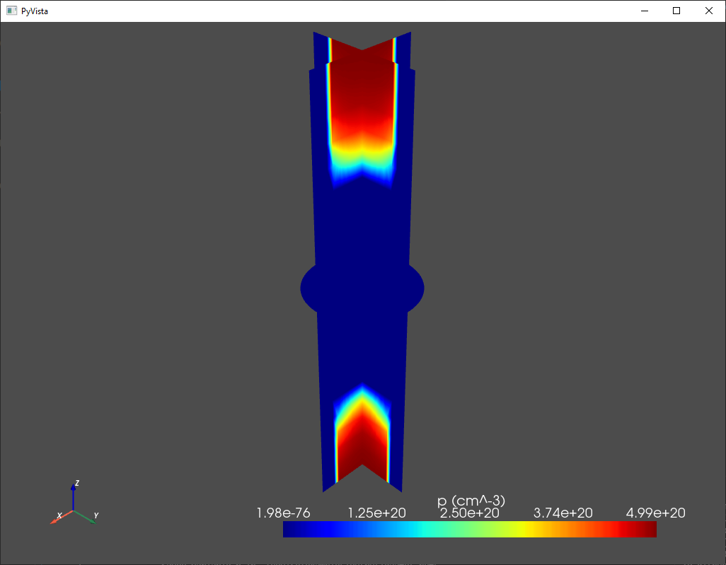
Fig. 2.4.3 Equilibrium hole density in the nanowire
By default, orthogonal slices are situated in the middle of the simulation
domain along each Cartesian direction. The location of the slices may however
be controlled with the 'x', 'y', and 'z' keyword arguments of the
plot_slices function. For more advanced data visualization, we recommend
that the user tries ParaView.
2.4.2. Postprocessing with ParaView
For postprocessing with ParaView, it is first necessary to save the quantities
to be visualized in .vtu format.
We first need to import the io module, which enables to save and load
files.
from qtcad.device import io
We then construct a dictionary that contains all the variables that we wish to visualize.
vars_dict = {"n": d.n/1e6, "p": d.p/1e6, "phi": d.phi,
   "EC": d.cond_band_edge()/ct.e, "EV": d.vlnce_band_edge()/ct.e}
The keys of the dictionary will correspond to the variable name once the output file is loaded into ParaView. In addition, here we divide densities by \(10^{6}\) to convert from SI base units into \(\textrm{cm}^{-3}\). We also divide the conduction and valence band edges by the fundamental electric charge to use eV units instead of Joules when plotting in ParaView.
The contents of the vars_dict dictionary, along with the mesh, may then
be saved with
path_vtu = script_dir / "nanowire.vtu"
io.save(path_vtu, vars_dict, mesh)
It is important to use the .vtu extension in the path for the io module
to recognize the format. Once the .vtu file is saved, it may be opened in
ParaView to benefit from its advanced plotting capabilities. More
information on ParaView may be found in Visualizing QTCAD® quantities with ParaView, or directly on
the ParaView website.
2.5. Code structure and workflow
To conclude, the following figure summarizes our workflow for QTCAD simulations.
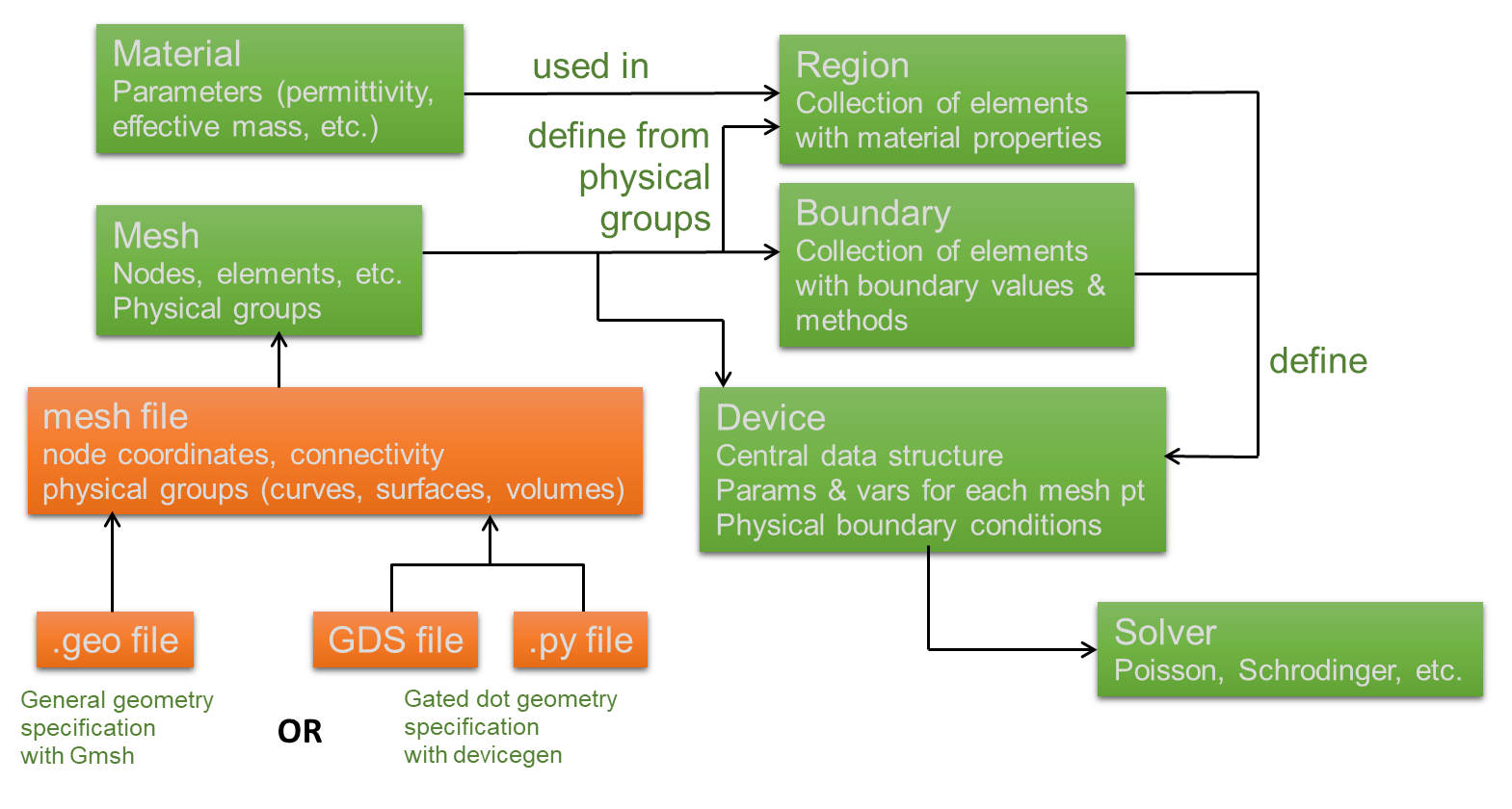
Fig. 2.5.1 Workflow for QTCAD simulations
The orange boxes represent features that are external to the Nanoacademic software, while the green boxes represent internal modules and classes. Together, these green boxes support the Python API for finite-element simulations.