1. Builder workflow: Ge/SiGe double quantum dot
1.1. Requirements
1.1.1. Software components
QTCAD®
1.1.2. Layout file
qtcad/examples/practical_application/Ge_hole/layouts/ge_dqd.oas
1.1.3. Python script
qtcad/examples/practical_application/Ge_hole/1-builder_ge.py
1.1.4. References
1.2. Briefing
As introduced in QTCAD Builder, the QTCAD Builder module streamlines the creation
of mesh files from a gate layout. Layouts can be imported from .gds or
.oas files generated by layout editors such as KLayout.
Alternatively, they can be constructed directly by creating polygons via built-in Builder commands.
The purpose of this tutorial is to demonstrate how Builder can be used to generate
meshes suitable for modeling spin-qubit devices within QTCAD.
Drawing inspiration from [HMM+24], we apply it to the
structure shown below.
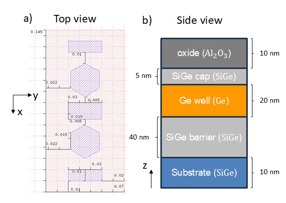
Fig. 1.2.1 Top and side views of the double-dot device under consideration
The left-hand side of the figure above shows the layout of the example device,
located at examples/practical_application/Ge_hole/layouts/gated_ge.oas.
The layout is provided in .oas format.
Following the procedure described in Gated Quantum Dot,
we assign a name property to each polygon in the .oas file and use these
names as references to the corresponding surfaces in the simulation setup. The blue rectangles
and hexagons represent metallic gates deposited on the chip surface. These gates
enable confinement of holes along the \(x\) and \(y\)
directions, while the heterostructure provides confinement in the \(z\) directions.
The right-hand side of the figure shows the heterostructure stack considered in this example.
1.3. Setup
1.3.1. Header
We begin by importing the required modules and defining the working directories.
From the builder module, we import the
Builder class to create an instance used to construct
the geometry from the two-dimensional layout provided in the .oas file.
We also import MeshAlgorithm3D, which provides access to
the different meshing algorithms available in the QTCAD Builder for generating a
3D mesh. These meshing algorithms will be discussed later in the meshing section
of this tutorial.
from qtcad.builder import Builder, MeshAlgorithm3D
from pathlib import Path

script_dir = Path(__file__).parent.resolve()
layout_dir = script_dir / "layout"
mesh_dir = script_dir / "meshes"
out_dir = script_dir / "output"
out_dir.mkdir(exist_ok=True)
1.3.2. Length scales and constants
We also define global mesh parameters and layer thicknesses.
# Mesh characteristic lengths
char_len = 5
dot_char_len = char_len / 2

# Thickness of each material layer (in nm)
high_k_gate = 10
SiGe_cap = 5
Ge_well = 20
SiGe_barrier = 40
substrate_thick = 10
1.4. Loading the layout
We begin by instantiating a Builder object and loading the .oas layout file using
the load_layout method. Once the layout has been imported,
the print_mask_tree method can be used to verify that the
masks and their associated polygons were loaded correctly.
At this stage, the Builder is initialized and connected to the geometry stored in the .oas layout file.
We use load_layout to import the ge_dqd.oas file and explicitly specify
cell_name="TOP" to load the top-level cell of the layout.
builder = Builder(name="Quantum Dot").load_layout(
    layout_dir / "ge_dqd.oas", cell_name="TOP"
)

builder.print_mask_tree()
Since load_layout automatically imports the top-level cell when cell_name
is not provided, specifying "TOP" is not strictly necessary here. We include it explicitly for clarity,
to indicate which cell is being loaded from the layout file.
The printed mask tree is shown below and provides an overview of the masks imported from the layout.
Layout
├── Mask 1 "dot-region"
│   └── 0  Polygon  "dot_region"
├── Mask 4 "gates"
│   ├── 0  Polygon  "P2"
│   ├── 1  Polygon  "P1"
│   ├── 2  Polygon  "BC"
│   ├── 3  Polygon  "BR"
│   └── 4  Polygon  "BL"
└── Mask 0 "substrate"
    └── 0  Polygon  "substrate"
This mask tree is consistent with the layer and polygon names defined in
the .oas layout file. In particular, the layout contains three masks
corresponding to the substrate, dot-region, and gate layers,
each containing the associated polygon objects.
The substrate mask contains a single polygon named substrate, which is used to
define and extrude the heterostructure stack. The dot-region mask contains the
polygon dot_region, which is later used to specify the quantum-dot region
for the hole simulation.
Finally, the gates mask contains all gate electrodes used in the device.
The polygons P1 and P2 correspond to the plunger gates, while BL,
BC, and BR denote the left, centre, and right barrier gates, respectively.
1.5. Building the heterostructure
We now construct the heterostructure by sequentially extruding layers
starting from the bottom of the substrate. The extrusion itself is performed using
the extrude method. Before calling this
method, we must identify the mask to extrude through the
use_mask method, which selects a layer from the .oas
layout file by name. In this context, a mask corresponds to a layout layer,
and all polygons contained in the selected mask are used during the extrusion process.
For each extrusion operation, we then define the name of the resulting 3D region
using set_group_name. Finally, we call
extrude, which takes the extrusion height as input
and generates the corresponding 3D volume from all polygons contained in the
currently selected mask.
This procedure, as shown below, is repeated for the substrate, silicon–germanium barrier, germanium well, silicon–germanium cap, and oxide layers to build the complete heterostructure.
(
    builder.set_mesh_size(char_len)
    .use_mask("substrate")
        # substrate
        .set_group_name("substrate")
        .extrude(substrate_thick)
        # SiGe barrier
        .set_group_name("SiGe_barrier")
        .extrude(SiGe_barrier)
        # ge well
        .set_group_name("Ge_well")
        .extrude(Ge_well)
        # sige cap
        .set_group_name("SiGe_cap")
        .extrude(SiGe_cap)
        # high-k gate
        .set_group_name("oxide")
        .extrude(high_k_gate)
)
After constructing the heterostructure, we can use the view
command to visualize it and save the resulting figure.
builder.view(
    surfaces=False,
    volume_labels=True,
    angles=(-90, 0, 85),
    save= str(out_dir / "heterostructure.svg"),
    zoom=1.1,
)
The command above generates a Gmsh instance that visualizes each individual component of the structure. The resulting figure shows the individual components of the structure, where each layer corresponds directly to a physical region of the Ge/SiGe heterostructure stack.
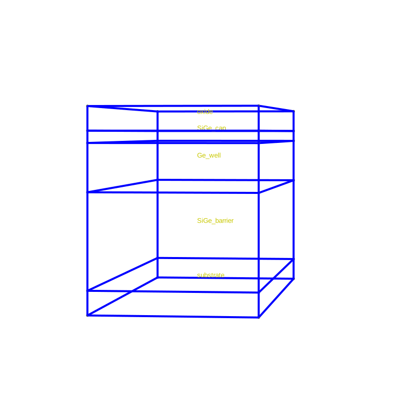
Fig. 1.5.6 Heterostructure stack generated with QTCAD Builder.
1.5.1. Building the dot region
Dot regions in QTCAD define the parts of the device where quantum confinement is expected. In these regions, carriers are not treated semiclassically but are instead described using the Schrödinger (and many-body) solvers.
To construct this region, we first determine its height from known layer thicknesses
and then define its starting position along the growth direction.
The get_z_from_group method is used only to retrieve
the position along \(z\) of the Ge_well layer, which serves as the anchor for
positioning the dot region.
In this case, the quantum-dot region is centered on the Ge_well layer and extended
into the surrounding SiGe_cap and SiGe_barrier layers to capture carrier
confinement. Specifically, half of the SiGe_cap and one-fifth of the SiGe_barrier
are included in the region.
The resulting dot height and starting position are defined as:
dot_height = Ge_well + SiGe_cap/2 + SiGe_barrier*(1/5)

starting_point = builder.get_z_from_group("Ge_well", bottom=True) \
                 - SiGe_barrier*(1/5)
We then use the dot-region mask to extrude the quantum-dot region from the
previously defined starting position and height. The extrusion is positioned
using set_z. Since this region will later be
treated with Schrödinger and many-body solvers, we assign a smaller mesh size
using set_mesh_size to obtain a higher-resolution
mesh compared to the surrounding regions of the device.
Because this operation involves overlaps with previously extruded volumes,
we enable overlay_mode, which assigns unique
labels to all intersecting regions. In particular, when two regions A and B
overlap, their intersection is automatically assigned the composite
name A.B. For additional details, see overlay_mode.
We now define the refined dot region:
(
    builder.set_z(starting_point)
        .overlay_mode()
        .set_mesh_size(dot_char_len)
        .use_mask("dot-region")
        .group_from_shape()
        .extrude(dot_height)
)
builder.view(
    surfaces=False,
    volume_labels=True,
    save=str(out_dir / "model_dr.svg"),
    zoom=1.1,
)
This region corresponds to where charge carriers (holes) are expected to be confined beneath the plunger gates.
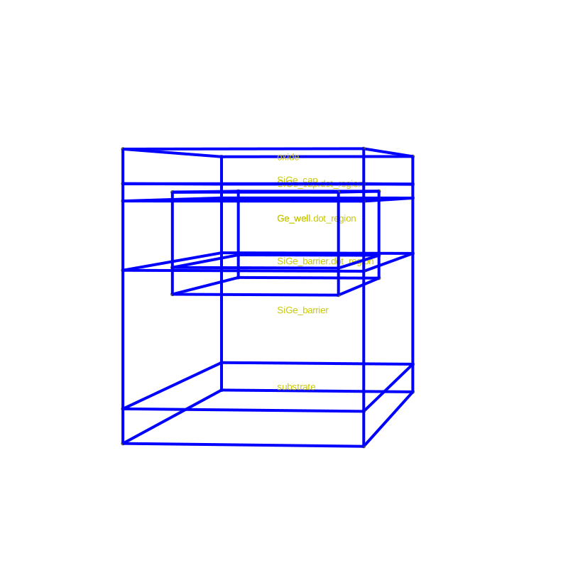
Fig. 1.5.7 Quantum-dot region.
1.6. Building the Gates
Next, we define the surfaces that will act as gates. The
gate electrodes from the gates mask are added as surfaces:
(
    builder.use_mask("gates")
        .displace_mode()
        .set_mesh_size(dot_char_len)
        .set_z_from_group("oxide")
        .group_from_shape()
        .add_surface()
)

builder.view(
    surface_labels=True,
    surfaces=True,
    angles=(0, 0, 0),
    save= str(out_dir / "surfs.svg"),
    zoom=1.2,
    groups=["BR","P1","P2","BC","BL",],
)
The P1 and P2 surfaces are plunger gates, while the BL, BR, and
BC surfaces are barrier gates. As discussed earlier, these names are
extracted from the name property of the corresponding polygons in the layout
(.oas) file.
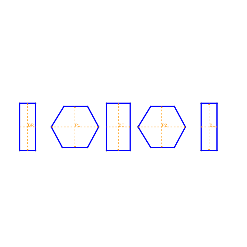
Fig. 1.6.1 Gate surfaces used for electrostatic control.
1.7. Generating the mesh
Finally, we generate the 3D mesh using the HXT algorithm. HXT is a
parallelized tetrahedral meshing algorithm (implemented in Gmsh)
that efficiently generates high-quality unstructured meshes for complex
device geometries, making it well-suited for large-scale simulations
with both coarse and finely resolved regions.
builder.mesh(3, algorithm3d=MeshAlgorithm3D.HXT, show_gmsh_output=True).write(
    mesh_dir / "ge_dqd.msh"
)
The geometry is also exported for later use:
builder.write(mesh_dir / "ge_dqd.xao")
Next, we generate visualization outputs of the full mesh and the dot region.
builder.view(
    surfaces=False,
    volume_labels=True,
    angles=(-90, 0, 85),
    save=str(out_dir /  "mesh.png"),
)

builder.view(
    surfaces=False,
    volume_labels=True,
    angles=(-90, 0, 85),
    save= str(out_dir / "mesh_dr.png"),
    groups=[
        "SiGe_barrier.dot_region",
        "Ge_well.dot_region",
        "SiGe_cap.dot_region",
    ],
)
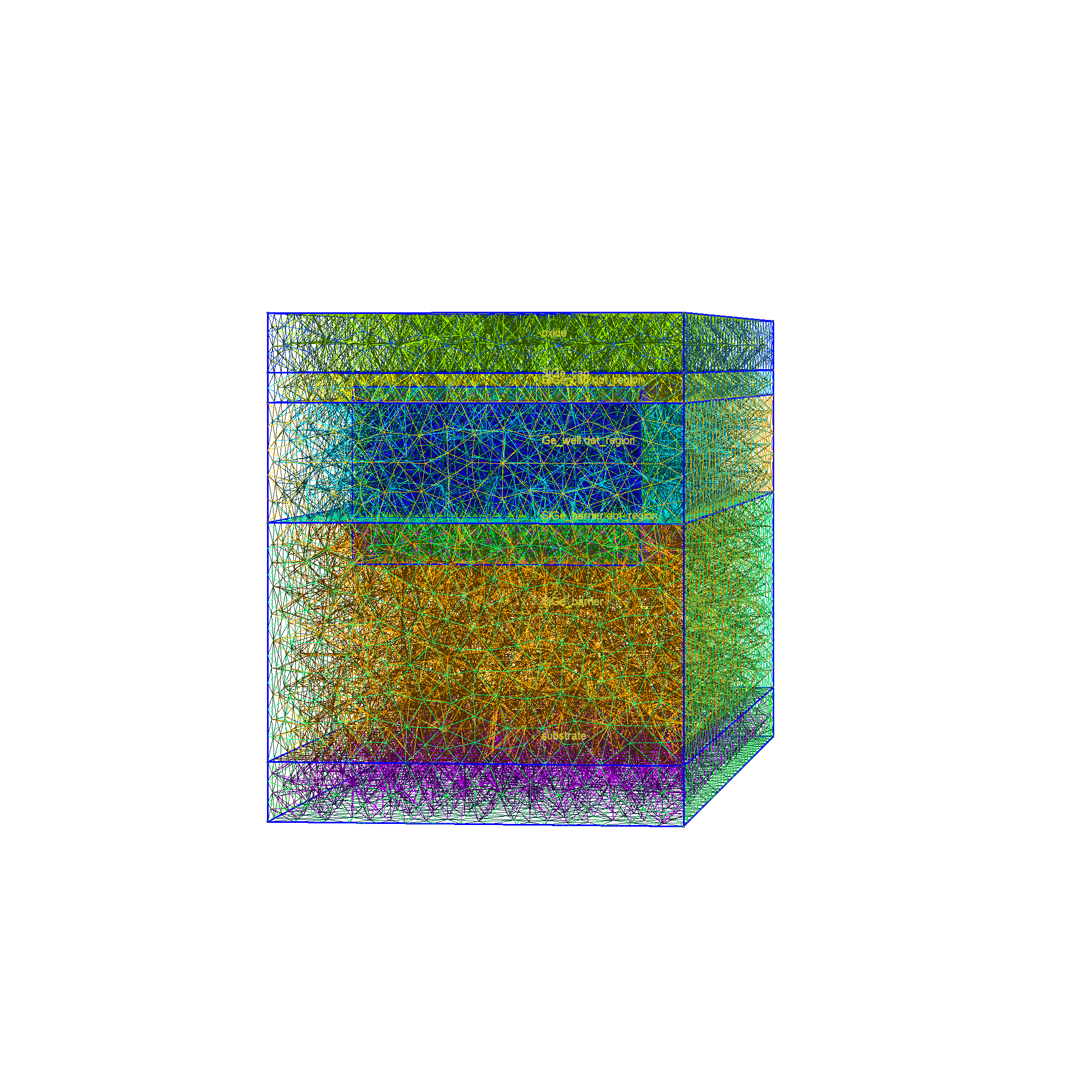
Fig. 1.7.5 Final 3D mesh of the device.
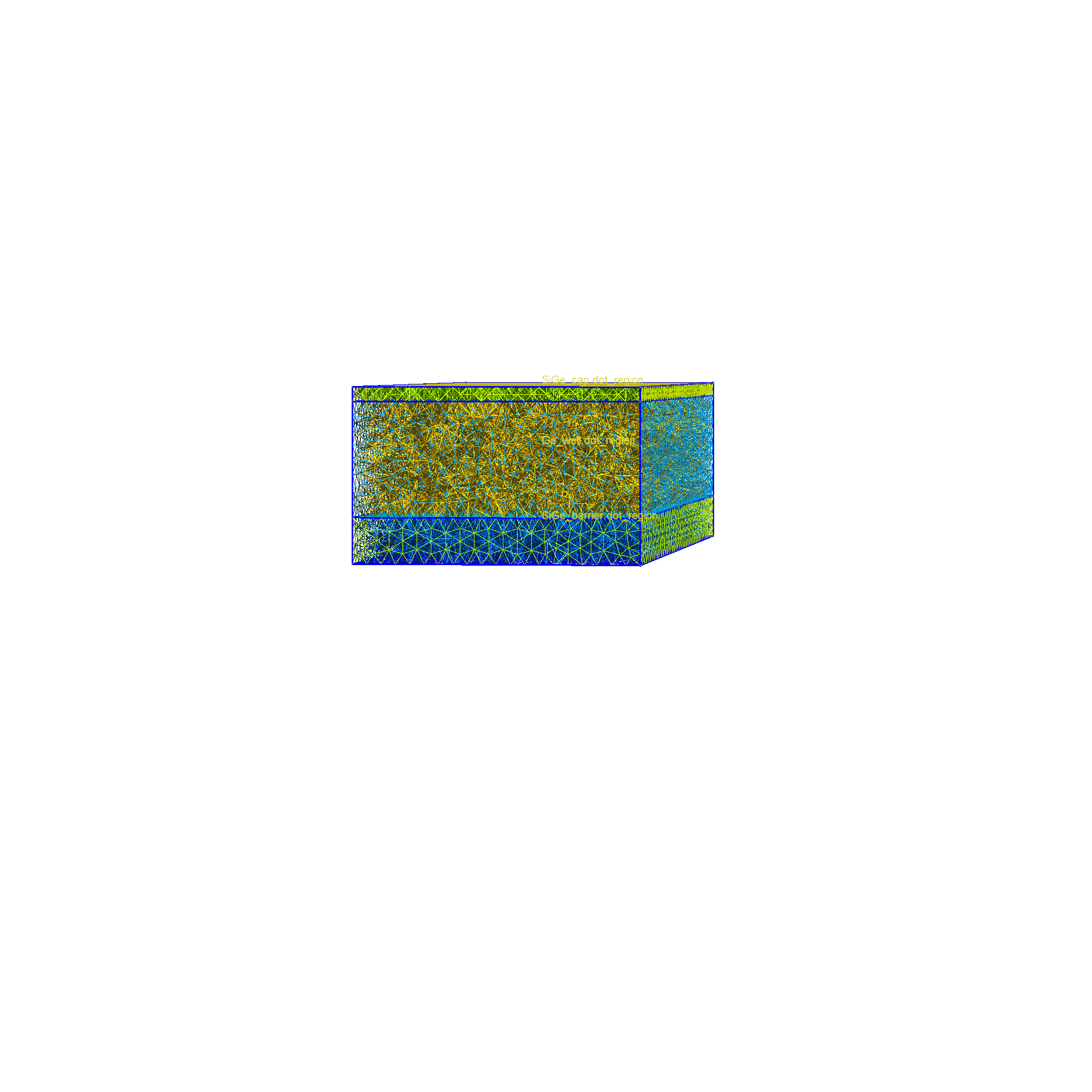
Fig. 1.7.6 Zoom on the quantum dot region.
1.8. Full code
__copyright__ = "Copyright 2022-2026, Nanoacademic Technologies Inc."

from qtcad.builder import Builder, MeshAlgorithm3D
from pathlib import Path

script_dir = Path(__file__).parent.resolve()
layout_dir = script_dir / "layout"
mesh_dir = script_dir / "meshes"
out_dir = script_dir / "output"
out_dir.mkdir(exist_ok=True)

# Mesh characteristic lengths
char_len = 5
dot_char_len = char_len / 2

# Thickness of each material layer (in nm)
high_k_gate = 10
SiGe_cap = 5
Ge_well = 20
SiGe_barrier = 40
substrate_thick = 10

builder = Builder(name="Quantum Dot").load_layout(
    layout_dir / "ge_dqd.oas", cell_name="TOP"
)

builder.print_mask_tree()

(
    builder.set_mesh_size(char_len)
    .use_mask("substrate")
    # substrate
    .set_group_name("substrate")
    .extrude(substrate_thick)
    # SiGe barrier
    .set_group_name("SiGe_barrier")
    .extrude(SiGe_barrier)
    # ge well
    .set_group_name("Ge_well")
    .extrude(Ge_well)
    # sige cap
    .set_group_name("SiGe_cap")
    .extrude(SiGe_cap)
    # high-k gate
    .set_group_name("oxide")
    .extrude(high_k_gate)
)

builder.view(
    surfaces=False,
    volume_labels=True,
    angles=(-90, 0, 85),
    save=str(out_dir / "heterostructure.svg"),
    zoom=1.1,
)

dot_height = Ge_well + SiGe_cap / 2 + SiGe_barrier * (1 / 5)

starting_point = builder.get_z_from_group("Ge_well", bottom=True) - SiGe_barrier * (
    1 / 5
)

(
    builder.set_z(starting_point)
    .overlay_mode()
    .set_mesh_size(dot_char_len)
    .use_mask("dot-region")
    .group_from_shape()
    .extrude(dot_height)
)
builder.view(
    surfaces=False,
    volume_labels=True,
    save=str(out_dir / "model_dr.svg"),
    zoom=1.1,
)

(
    builder.use_mask("gates")
    .displace_mode()
    .set_mesh_size(dot_char_len)
    .set_z_from_group("oxide")
    .group_from_shape()
    .add_surface()
)

builder.view(
    surface_labels=True,
    surfaces=True,
    angles=(0, 0, 0),
    save=str(out_dir / "surfs.svg"),
    zoom=1.2,
    groups=[
        "BR",
        "P1",
        "P2",
        "BC",
        "BL",
    ],
)

builder.mesh(3, algorithm3d=MeshAlgorithm3D.HXT, show_gmsh_output=True).write(
    mesh_dir / "ge_dqd.msh"
)

builder.write(mesh_dir / "ge_dqd.xao")


builder.view(
    surfaces=False,
    volume_labels=True,
    angles=(-90, 0, 85),
    save=str(out_dir / "mesh.png"),
)

builder.view(
    surfaces=False,
    volume_labels=True,
    angles=(-90, 0, 85),
    save=str(out_dir / "mesh_dr.png"),
    groups=[
        "SiGe_barrier.dot_region",
        "Ge_well.dot_region",
        "SiGe_cap.dot_region",
    ],
)