2. Simulating hole states in a Ge/SiGe quantum dot using Poisson and Schrödinger solvers
2.1. Requirements
2.1.1. Software components
QTCAD®
2.1.2. Mesh file
qtcad/examples/practical_application/Ge_hole/layouts/ge_dqd.msh
2.1.3. Python script
qtcad/examples/practical_application/Ge_hole/1-poisson_schrod.py
2.1.4. References
2.2. Briefing
In the previous tutorial, we constructed a Ge/SiGe heterostructure and generated a mesh using the QTCAD Builder workflow.
In this tutorial, we simulate a double quantum dot device by:
Solving the nonlinear Poisson equation to obtain the electrostatic potential;
Solving the Schrödinger equation to compute bound hole states.
This work uses a realistic device architecture similar to that reported in [HMM+24].
2.3. Setting up the device
2.3.1. Header
We begin by importing the required modules.
from qtcad.device import constants as ct
from qtcad.device import materials as mt
from qtcad.device import io

from qtcad.device.mesh3d import Mesh, SubMesh
from qtcad.device import Device, SubDevice

from qtcad.device.poisson import Solver as PoissonSolver
from qtcad.device.poisson import SolverParams as PoissonSolverParams

from qtcad.device.schrodinger import Solver as SchrodingerSolver
from qtcad.device.schrodinger import SolverParams as SchrodingerSolverParams

from qtcad.device import analysis as an

import numpy as np
from pathlib import Path
from matplotlib import pyplot as plt
2.3.2. Loading the mesh
We then define the paths to the mesh and geometry
files (.msh and .xao) we previously generated in Builder workflow: Ge/SiGe double quantum dot.
script_dir = Path(__file__).parent.resolve()
mesh_dir = script_dir / "meshes"
mesh_file_dir = mesh_dir / "ge_dqd.msh"
xao_dir = mesh_dir / "ge_dqd.xao"
out_dir = script_dir / "output"
out_dir.mkdir(exist_ok=True)
The mesh is then loaded with nanometer scaling.
scaling = 1e-9  # nanometers
mesh = Mesh(scaling, mesh_file_dir)
mesh.show()
The scaling factor specifies that distances in the .msh file are expressed
in nanometers.
2.3.3. Building the device
We construct the device by passing the previously created
Mesh object, which defines the
device geometry and discretization.
Next, we specify the physical model used for the confined carriers. Since we consider hole states, we employ a four-band \(\mathbf{k} \cdot \mathbf{p}\) description based on the Luttinger–Kohn–Foreman formulation (see k.p module for details and references).
dvc = Device(mesh, conf_carriers='h',
             hole_kp_model="luttinger_kohn_foreman")

dvc.set_temperature(0.1)
Next, we assign the device temperature using the
set_temperature method.
When solving the nonlinear Poisson equation later in this workflow, the assigned
temperature is used to determine the charge density and electrostatic
potential. For more details, see Poisson solvers.
2.3.4. Assigning materials to regions
For each region specified in a heterostructure stack, we assign the corresponding material.
In this example, we use SiGe_DFT and Ge_strained_on_SiGe, along with other standard
materials introduced previously.
The SiGe_DFT and Ge_strained_on_SiGe material parameters were obtained
from atomistic first-principles simulations performed in Nanoacademic
Technologies’s density-functional theory package, RESCU.
They provide an accurate description of Ge/SiGe heterostructures,
particularly in terms of band alignment and strain effects.
# Assign the material to regions
dvc.new_region("substrate", mt.SiGe_DFT)
dvc.new_region("SiGe_barrier", mt.SiGe_DFT)
dvc.new_region("Ge_well", mt.Ge)
dvc.new_region("SiGe_cap", mt.SiGe_DFT)
dvc.new_region("oxide", mt.Al2O3)

# Dot-region volumes
dvc.new_region("Ge_well.dot_region", mt.Ge)
dvc.new_region("SiGe_barrier.dot_region", mt.SiGe_DFT)
dvc.new_region("SiGe_cap.dot_region", mt.SiGe_DFT)
2.3.5. Boundary conditions
Next, we apply the gate voltages through boundary conditions.
# boundary conditions
Ew = mt.Ge.chi + 1.1*mt.Ge.Eg
dvc.new_gate_bnd("P1", -0.6, Ew)
dvc.new_gate_bnd("P2", -0.6, Ew)
dvc.new_gate_bnd("BC", 0.9, Ew)
dvc.new_gate_bnd("BL", 0.5, Ew)
dvc.new_gate_bnd("BR", 0.5, Ew)
These gates define the electrostatic confinement of the double quantum dot.
2.3.6. Visualization
To visualize the device, we can use the built-in QTCAD visualizer via the
show method of the device object. This
will open an interactive viewer in a browser window.
# visualize
dvc.show()
The viewer allows you to inspect the geometry, including individual regions (volumes) and boundary surfaces of the simulated device.
A window similar to the one shown in the figure below will be displayed.
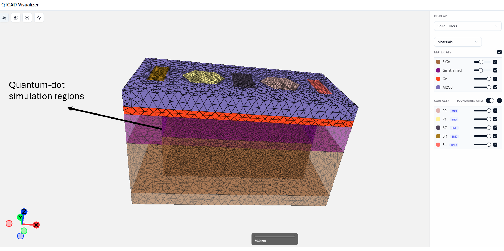
Fig. 2.3.4 QTCAD visualizer window illustrating the device geometry and gate layout.
2.4. Solving the nonlinear Poisson equation
Before initializing the nonlinear Poisson Solver,
we first define the quantum-dot region. This region is expected to host the confined hole
states and is therefore treated quantum mechanically.
As a result, classical charge is excluded from this region in the Poisson solver. The electrostatic potential is computed self-consistently throughout the device, and the quantum dot region will later be treated using the Schrödinger (and many-body) solvers.
dot_region_list = [
    "Ge_well.dot_region",
    "SiGe_barrier.dot_region",
    "SiGe_cap.dot_region"
]

dvc.set_dot_region(dot_region_list)
2.4.1. Poisson solver setup
We now specify the Poisson solver parameters using the
SolverParams class from
the Poisson module.
poisson_params = PoissonSolverParams()
poisson_params.tol = 1e-3
poisson_params.maxiter = 50
poisson_params.refined_region = dot_region_list
poisson_params.h_refined = 1.5
poisson_params.initial_ref_factor = 0.1
poisson_params.final_ref_factor = 0.75
poisson_params.refined_mesh_filename = mesh_dir / "refined_gedqd.msh"
We then initialize the Solver. In this
example, adaptive mesh refinement is enabled by providing the geometry file
(.xao). Because adaptive meshing is used, several settings are specified
in the SolverParams class to
control and tune the refinement procedure. For additional details, see the
existing adaptive meshing tutorial.
The refined mesh is then stored as refined_gedqd.msh and used in later tutorials.
poisson_solver = PoissonSolver(
    dvc,
    solver_params=poisson_params, geo_file=xao_dir

)
The solver computes the electrostatic potential self-consistently throughout the device, taking into account material properties, boundary conditions, and carrier statistics.
poisson_solver.solve()
The resulting electrostatic potential is stored in the device attribute
phi (API
documentation) and is also saved to an .hdf5 file for use in subsequent simulations.
io.save(out_dir / 'electrostatic_potential.hdf5', dvc.phi)
2.4.2. Analyzing the electrostatic potential
Once the Poisson solver has converged, we can analyze the resulting
electrostatic potential stored in the Device.
We extract a 1D line cut through the device to examine the band profile more closely.
begin=(-20e-9, 35e-9, 60e-9)
end=(125e-9, 35e-9, 60e-9)

an.plot_bands(dvc, begin, end,
              show_figure=True,
              path=out_dir / "band_edges_linecut.png")
The line cut is chosen to pass through the quantum dot region, allowing us to inspect the variation of the band edges in this region.
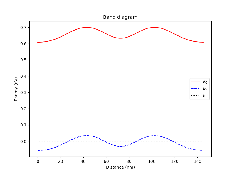
Fig. 2.4.11 Band edge profile along a line cut through the quantum dot region.
In particular, the valence band edge profile provides insight into hole confinement: regions where the valence band edge reaches local maxima form potential wells in which hole states can become localized.
Next, to visualize the valence band edge profile more clearly, we extract the
valence band edge values across the entire device using the
vlnce_band_edge method. We then use the
linecut function from the analysis
module to extract a linecut between specified start and end points within the 3D device geometry.
Finally, we use the Python library matplotlib to plot the valence band edge along the selected line.
x_cords, val_cut = an.linecut(dvc.mesh, dvc.vlnce_band_edge(), begin, end)
fig, ax = plt.subplots()
ax.plot(x_cords*1e9, val_cut/ct.e, label="Valence band edge (eV)")
ax.axhline(0, color='k', linestyle='--', label="Fermi level")
ax.set_xlabel("x (nm)")
ax.set_ylabel("Energy (eV)")
ax.set_title("Valence band edge along line cut")
ax.legend()
fig.savefig(out_dir / "valence_band_linecut.png")
plt.show()
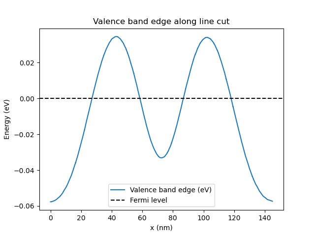
Fig. 2.4.12 Valence band edge profile along a line cut through the quantum dot region.
2.5. Solving the Schrödinger equation
After solving the Poisson equation, we focus on the quantum dot region and solve the single-body Schrödinger equation for holes.
We first compute the confinement potential from the electrostatic potential using the following command.
dvc.set_V_from_phi()
Next, we construct a SubMesh and a
SubDevice that encompass the quantum-dot
region, where the classical charge has been set to zero. The Schrödinger equation
is then solved within this region by passing the
SubDevice to the solver.
submesh = SubMesh(dvc.mesh, dot_region_list)
subdvc = SubDevice(dvc, submesh)
2.5.1. Schrödinger solver setup
Finally, we specify the number of states to be resolved by the Schrödinger solver and solve the equation on the subdevice.
schrodinger_params = SchrodingerSolverParams()
schrodinger_params.num_states = 6

schrodinger_solver = SchrodingerSolver(subdvc,
    solver_params=schrodinger_params)
schrodinger_solver.solve()
The solver computes the bound-state energies and wavefunctions
of holes confined in the quantum-dot. The resulting energies are
stored in the subdevice attribute energies,
while the corresponding eigenfunctions are stored in
eigenfunctions
(API documentation).
For holes, the eigenfunctions are represented as a 3D array, where the first index corresponds to the global nodes of the mesh, the second to the energy level, and the third index runs over the bands of the Luttinger–Kohn–Foreman model.
2.5.2. Results and analysis
We now extract and analyze the computed eigenstates from the Schrödinger solver. This includes printing the energy spectrum and performing a basic analysis of the quantum dot geometry.
subdvc.print_energies()
an.analyze_dot(subdvc, verbose=True)
This produces the following output:
Energy levels (eV)
[-0.03976152 -0.03976138 -0.03926827 -0.03926812 -0.03341363 -0.03341297]
--------------------------------------------------------------------------------
Geometric properties of the quantum dot:
--------------------------------------------------------------------------------
position        :  [2.29419510e-08 3.48701068e-08 6.57439006e-08]
std             :  [4.27572602e-09 5.24526878e-09 2.43138577e-09]
size            :  [1.71029041e-08 2.09810751e-08 9.72554306e-09]
--------------------------------------------------------------------------------
Next, we access the computed eigenfunctions and construct the probability density. The wavefunctions are squared and summed over bands to obtain the probability density field for visualization.
psi = subdvc.eigenfunctions
psi2 = np.sum(np.abs(psi) ** 2, axis=2)
We then plot slices of the ground-state probability density and save the
result to .png files.
an.plot_slices(
    subdvc.mesh,
    psi2[:, 0],
    title="Ground state |psi|^2",
    show_figure=False,
    path=out_dir / "Ge_Ground_state.png",
)
an.plot_slices(
    subdvc.mesh,
    psi2[:, 1],
    title="First excited state |psi|^2",
    show_figure=False,
    path=out_dir / "Ge_First_excited_state.png",
)
an.plot_slices(
    subdvc.mesh,
    psi2[:, 2],
    title="Second excited state |psi|^2",
    show_figure=False,
    path=out_dir / "Ge_Second_excited_state.png",
)
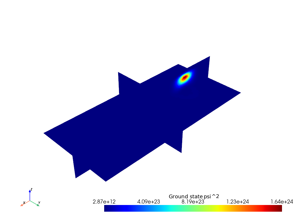
Fig. 2.5.5 Ground state probability density.

Fig. 2.5.6 First-excited-state probability density.
Examining the energy levels and eigenfunctions of the ground and first-excited states shows that they form a degenerate pair. This degeneracy is the expected Kramers degeneracy of the Luttinger–Kohn–Foreman Hamiltonian: in the absence of magnetic fields or other time-reversal-symmetry-breaking terms, each confined hole state has a time-reversed partner with the same energy.

Fig. 2.5.7 Second-excited-state probability density.
2.6. Full code
__copyright__ = "Copyright 2022-2026, Nanoacademic Technologies Inc."

from qtcad.device import constants as ct
from qtcad.device import materials as mt
from qtcad.device import io
from qtcad.device.mesh3d import Mesh, SubMesh
from qtcad.device import Device, SubDevice
from qtcad.device.poisson import Solver as PoissonSolver
from qtcad.device.poisson import SolverParams as PoissonSolverParams
from qtcad.device.schrodinger import Solver as SchrodingerSolver
from qtcad.device.schrodinger import SolverParams as SchrodingerSolverParams
from qtcad.device import analysis as an
import numpy as np
from pathlib import Path
from matplotlib import pyplot as plt

script_dir = Path(__file__).parent.resolve()
mesh_dir = script_dir / "meshes"
mesh_file_dir = mesh_dir / "ge_dqd.msh"
xao_dir = mesh_dir / "ge_dqd.xao"
out_dir = script_dir / "output"
out_dir.mkdir(exist_ok=True)

scaling = 1e-9  # nanometers
mesh = Mesh(scaling, mesh_file_dir)
mesh.show()

dvc = Device(mesh, conf_carriers="h", hole_kp_model="luttinger_kohn_foreman")

dvc.set_temperature(0.1)

# Assign the material to regions
dvc.new_region("substrate", mt.SiGe_DFT)
dvc.new_region("SiGe_barrier", mt.SiGe_DFT)
dvc.new_region("Ge_well", mt.Ge)
dvc.new_region("SiGe_cap", mt.SiGe_DFT)
dvc.new_region("oxide", mt.Al2O3)

# Dot-region volumes
dvc.new_region("Ge_well.dot_region", mt.Ge)
dvc.new_region("SiGe_barrier.dot_region", mt.SiGe_DFT)
dvc.new_region("SiGe_cap.dot_region", mt.SiGe_DFT)

# boundary conditions
Ew = mt.Ge.chi + 1.1 * mt.Ge.Eg
dvc.new_gate_bnd("P1", -0.6, Ew)
dvc.new_gate_bnd("P2", -0.6, Ew)
dvc.new_gate_bnd("BC", 0.9, Ew)
dvc.new_gate_bnd("BL", 0.5, Ew)
dvc.new_gate_bnd("BR", 0.5, Ew)

# visualize
dvc.show()

dot_region_list = [
    "Ge_well.dot_region",
    "SiGe_barrier.dot_region",
    "SiGe_cap.dot_region",
]

dvc.set_dot_region(dot_region_list)

poisson_params = PoissonSolverParams()
poisson_params.tol = 1e-3
poisson_params.maxiter = 50
poisson_params.refined_region = dot_region_list
poisson_params.h_refined = 1.5
poisson_params.initial_ref_factor = 0.1
poisson_params.final_ref_factor = 0.75
poisson_params.refined_mesh_filename = mesh_dir / "refined_gedqd.msh"

poisson_solver = PoissonSolver(dvc, solver_params=poisson_params, geo_file=xao_dir)

poisson_solver.solve()

io.save(out_dir / "electrostatic_potential.hdf5", dvc.phi)

begin = (-20e-9, 35e-9, 60e-9)
end = (125e-9, 35e-9, 60e-9)

an.plot_bands(
    dvc, begin, end, show_figure=True, path=out_dir / "band_edges_linecut.png"
)

x_cords, val_cut = an.linecut(dvc.mesh, dvc.vlnce_band_edge(), begin, end)
fig, ax = plt.subplots()
ax.plot(x_cords * 1e9, val_cut / ct.e, label="Valence band edge (eV)")
ax.axhline(0, color="k", linestyle="--", label="Fermi level")
ax.set_xlabel("x (nm)")
ax.set_ylabel("Energy (eV)")
ax.set_title("Valence band edge along line cut")
ax.legend()
fig.savefig(out_dir / "valence_band_linecut.png")
plt.show()

dvc.set_V_from_phi()

submesh = SubMesh(dvc.mesh, dot_region_list)
subdvc = SubDevice(dvc, submesh)

schrodinger_params = SchrodingerSolverParams()
schrodinger_params.num_states = 6

schrodinger_solver = SchrodingerSolver(subdvc, solver_params=schrodinger_params)
schrodinger_solver.solve()

subdvc.print_energies()
an.analyze_dot(subdvc, verbose=True)

psi = subdvc.eigenfunctions
psi2 = np.sum(np.abs(psi) ** 2, axis=2)

an.plot_slices(
    subdvc.mesh,
    psi2[:, 0],
    title="Ground state |psi|^2",
    show_figure=False,
    path=out_dir / "Ge_Ground_state.png",
)
an.plot_slices(
    subdvc.mesh,
    psi2[:, 1],
    title="First excited state |psi|^2",
    show_figure=False,
    path=out_dir / "Ge_First_excited_state.png",
)
an.plot_slices(
    subdvc.mesh,
    psi2[:, 2],
    title="Second excited state |psi|^2",
    show_figure=False,
    path=out_dir / "Ge_Second_excited_state.png",
)