4. NEGF–Poisson simulations of an FD-SOI field-effect transistor with a quantum dot
4.1. Requirements
4.1.1. Software components
QTCAD
Gmsh
4.1.2. Geometry file
qtcad/examples/tutorials/meshes/fdsoi_negf.geo
4.1.3. Python script
qtcad/examples/tutorials/fdsoi_negf.py
4.1.4. References
4.2. Briefing
In this tutorial, we will demonstrate how to simulate the nonequilibrium quantum statistics and quantum transport phenomena arising in a field-effect transistor (FET) subject to a finite drain–source bias. Specifically, the simulated device has a fully-depleted silicon-on-insulator (FD-SOI) geometry and includes a quantum dot whose confinement potential is defined using three metallic top gates.
The device’s electrostatics are solved for by self-consistently computing the charge density using the nonequilibrium Green’s function formalism (NEGF) and the electric potential using Poisson’s equation; the simulation is therefore referred to as an “NEGF–Poisson” simulation. Quantum transport phenomena and the drain–source current are then modeled via the Landauer–Büttiker formula.
We will focus on three of the main physical regimes of transport through such a device: transport in the off state, transport in the sequential tunneling regime, and transport in the on state.
4.3. Device geometry
Not unlike the FD-SOI FET presented in A double quantum dot device in a fully-depleted silicon-on-insulator transistor, the device considered in this tutorial consists of a silicon nanosheet with a rectangular cross section entirely surrounded by silicon dioxide. The silicon nanosheet has a width of \(10~\textrm{nm}\) and a thickness of \(3~\textrm{nm}\). It is partitioned into three regions: a degenerately-n-doped source, an intrinsic channel, and a degenerately-n-doped drain.
The silicon dioxide layer on top of the nanosheet has a thickness of \(2~\textrm{nm}\). The top surface of the top oxide includes three metallic gates that define the confinement potential of a quantum dot in the middle of the silicon nanosheet channel: two barrier gates and one plunger gate, as shown below.
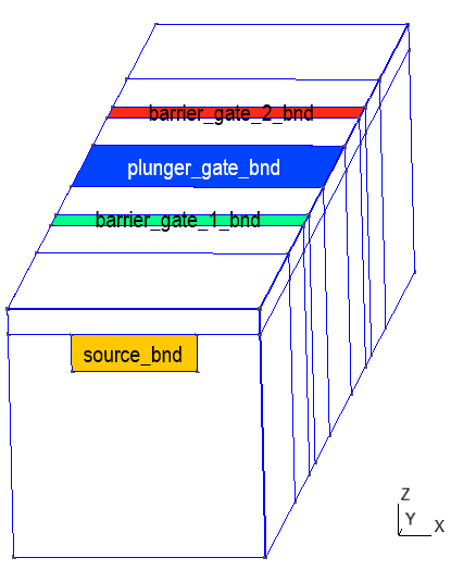
Fig. 4.3.1 Labeled boundaries of the FD-SOI FET considered in this tutorial highlighting the top gates and the source contact.
The silicon dioxide layer below the silicon nanosheet (namely the buried oxide) has a thickness of \(15~\textrm{nm}\). Later in this tutorial, a frozen boundary condition will be applied on the bottom surface of this buried oxide to model body biasing through a back gate, as was done in A double quantum dot device in a fully-depleted silicon-on-insulator transistor; this back gate boundary is shown below.
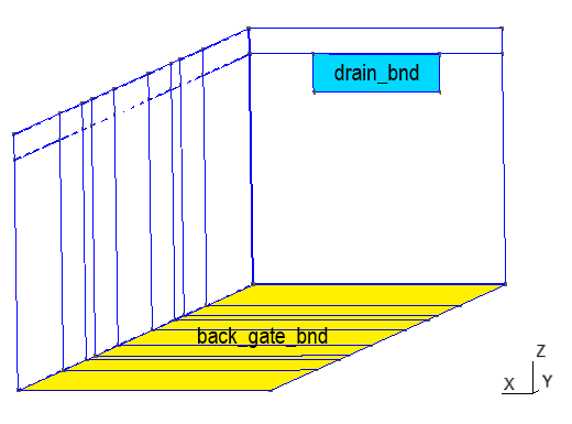
Fig. 4.3.2 Labeled boundaries of the FD-SOI FET considered in this tutorial highlighting the back gate and the drain contact.
4.4. Mesh construction—Requirements for NEGF simulations
Inspecting the mesh file for the device considered in this tutorial located at
qtcad/examples/tutorials/meshes/fdsoi_negf.geo, it may be noted that all
volumes of the mesh are constructed through extrusions along the \(y\)
axis, namely the transport direction (or source–drain direction). For example,
the volume defining the source of the silicon nanosheet is defined as follows.
extrusion_si[] = Extrude {0, l_source, 0} {Surface{1}; Layers{layers_source};};
This method of mesh construction ensures that the global nodes of the mesh may be partitioned into layers of nodes that form planes normal to the transport direction. Furthermore, the global nodes in each such layer are connected through elements only to the global nodes in two neighboring layers. Finally, the layers all have the same number of global nodes. For technical reasons, such meshes greatly reduce the computational burden of NEGF simulations. The QTCAD NEGF module therefore requires meshes to be constructed through extrusions along the transport direction.
4.5. Setting up the device
4.5.1. Header
We start by importing the various modules, classes, and functions which will be used for the simulation.
import pathlib
from os import cpu_count

import numpy as np

from qtcad.device import constants as ct
from qtcad.device.mesh3d import Mesh, SubMesh
from qtcad.device import materials as mt
from qtcad.device import Device, SubDevice
from qtcad.transport.negf_poisson import Solver, SolverParams
Most of these have been seen before, with the following exceptions:
os.cpu_count: A function which returns the number of logical CPUs (cores) available on the system. Due to the relatively heavy computational burden of NEGF simulations, parallelization is crucial. This method will help determine the number of cores over which the computation can be parallelized.
transport.negf_poisson: A QTCAD module containing the two classes required for an NEGF–Poisson simulation:
SolverandSolverParams, which serve similar roles as the classes with the same names in other QTCAD modules such as thedevice.poissonmodule.
4.5.2. Loading the mesh
As usual, the mesh is then loaded from the appropriate .geo file in the
mesh folder.
# Set up paths
script_dir = pathlib.Path(__file__).parent.resolve()
path_mesh = script_dir / "meshes"
path_out = script_dir / "output"

# Load the mesh
scaling = 1e-9
mesh = Mesh(scaling, str(path_mesh / "fdsoi_negf.msh"))
Note that we have also defined the path to the folder in which simulation
outputs will be saved, path_out.
4.5.3. Defining material composition and doping in the device
A device d is then defined from the mesh that we just loaded.
# Define the device object
d = Device(mesh, conf_carriers='e')
d.set_temperature(0.1)
Here, the device attribute conf_carriers has been set to 'e'. In the
context of NEGF–Poisson simulation, this means that the only charges under
consideration are (1) dopants and (2) electrons whose charge density is to be
computed within the NEGF formalism. In particular, any charge density arising
from holes as well as the classical electron density are ignored (including in
the doped source and drain—see Eq. (11.5)).
Also note that the temperature has been set to \(0.1~\textrm{K}\). Since the NEGF formalism captures quantum-mechanical effects, such as the Heisenberg uncertainty principle, charge density profiles computed within the NEGF formalism are relatively spread-out. This is to be contrasted to the charge density profiles computed within semiclassical semiconductor statistics, as in the QTCAD non-linear Poisson solver, which tend to exhibit sharp variations wherever the band edge crosses the Fermi level; this phenomenon is exacerbated at cryogenic temperatures. As such, the convergence of NEGF–Poisson simulations is fairly unaffected by temperature; NEGF–Poisson simulations can converge at very low temperatures, even on a very coarse mesh. In particular, this means that adaptive meshing is not required to ensure convergence of NEGF–Poisson simulations, even at sub-Kelvin temperatures. In this tutorial, to reduce computation time, we use a relatively coarse mesh. However, the final results of this tutorial would likely differ had we used a finer mesh instead.
The various volumes of the device are then assigned a material and a doping concentration.
# Create the regions
ndoping = 2e20 * 1e6
d.new_region("top_ox", mt.SiO2_ideal)
d.new_region("source", mt.Si, ndoping=ndoping)
d.new_region("channel", mt.Si)
d.new_region("drain", mt.Si, ndoping=ndoping)
d.new_region("side_bot_ox", mt.SiO2_ideal)
4.5.4. Boundary condition on the back gate
We then set a frozen boundary condition on the back gate, mimicking A double quantum dot device in a fully-depleted silicon-on-insulator transistor. In a nutshell, this type of boundary condition ensures that the Fermi level is pinned halfway between the conduction band edge and the donor level.
# Set up boundary condition for back gate
back_gate_bias = -0.2
doping_back_gate = 1e15 * 1e6
binding_energy = 46 * 1e-3 * ct.e
d.new_frozen_bnd("back_gate_bnd", back_gate_bias, mt.Si, doping_back_gate,
   "n", binding_energy)
4.6. NEGF-specific simulation parameters
The structure of the code presented so far in this tutorial bears no qualitative difference with that of other kinds of simulations which may be performed within QTCAD. We now come to simulation parameters specific to NEGF simulations.
All QTCAD NEGF simulations require exactly two labeled surfaces to be assigned
a “quantum lead” boundary condition, as may be done using the
new_quantum_lead_bnd
method of the Device class. These
boundaries correspond to the interfaces with the source and drain leads, which,
in the NEGF formalism, are assumed to be thermal baths from which charge
carriers may be emitted and into which charge carriers may be absorbed. This
method takes two inputs, the first of which is the appropriate boundary label
which was defined when constructing the mesh in Gmsh
(here, "source_bnd" and "drain_bnd"), and the second of which sets
whether an essential boundary condition (essential=True) or a natural
boundary condition (essential=False) is assumed. For quantum lead boundary
conditions, it is recommended to assume natural boundary conditions
(essential=False) whenever possible, in particular for any device that has
at least one essential boundary (such as a gate).
# Set boundary conditions for source and drain of FET for NEGF simulation
d.new_quantum_lead_bnd("source_bnd", essential=False)
d.new_quantum_lead_bnd("drain_bnd", essential=False)
Vds = 0.05 # drain-to-source voltage
Note that we have also defined Vds, the drain–source voltage, to be equal
to \(50~\textrm{mV}\). This parameter will be used later.
Next, we define a subdevice corresponding to the silicon nanosheet, and store
it to a variable named d_negf.
# Restrict calculation of charge density on a subdevice
submesh = SubMesh(mesh, ["source", "channel", "drain"])
d_negf = SubDevice(d, submesh)
Later, the calculation of the charge density within the NEGF formalism will be
restricted to d_negf to reduce computational burden. It is also worth
noting that the electron density on the boundaries of d_negf will be set to
zero. This is because d_negf, which represents the entirety of the silicon
nanosheet, is entirely surrounded by an ideal oxide, SiO2_ideal; see
Boundary conditions.
NEGF-Poisson solver parameters
are then defined.
# NEGF-Poisson solver parameters
solver_params = SolverParams()
# Compute NEGF at different energy values in parallel
if cpu_count() >= 4:
   n_jobs = 4
else:
   n_jobs = 1
solver_params.n_jobs = n_jobs
mixing_param = [0.05, 0.05, 0.02]
We note that by default, SolverParams().adaptive is set to True;
see API reference. This
solver parameter, adaptive, plays an important role in the calculation of
charge density. Specifically, within the NEGF formalism, this calculation
involves the integration of a Green’s function over
energy (see Eq. (11.4)). This Green’s function is commonly highly
ill-behaved; it may exhibit singularities and discontinuities. Thus, to ensure
that such Green’s functions are accurately integrated (thereby leading to
accurate calculations of charge density), Nanoacademic Technologies has
developed an adaptive integration algorithm well-suited for the NEGF context.
In turn, adaptive integration plays an important role in the convergence of
NEGF–Poisson simulations. Indeed, adaptive integration enables consistently
accurate evaluations of charge density across iterations of the NEGF–Poisson
algorithm. In contrast, non-adaptive integration (i.e. integration under a
fixed quadrature) may lead to inaccuracies in charge density that in turn may
lead to erratic variations in electric potential.
We alter the default solver-parameter values defined through
SolverParams
in two ways. First, an attribute pertaining to parallelization is set. The
evaluations of a Green’s function at multiple values of energy required to
compute the charge density (see Eq. (11.4)) may be performed in
parallel. The number of concurrent Green’s function evaluations is set through
solver_params.n_jobs, which we set to 4 if the computer has at least
four logical cores and to 1 otherwise. This is to ensure the results of
this tutorial are consistent across machines, since the adaptive
integration algorithm behaves slightly differently depending on the value of
solver_params.n_jobs. Second, we define three mixing parameters (one for
each investigated regime of quantum transport) and store them in the list
mixing_param; these parameters pertain to the convergence of NEGF–Poisson
simulations and will be discussed in the next section.
4.7. NEGF–Poisson simulation and postprocessing
We are now nearly ready to set up NEGF–Poisson solvers to investigate the operation of our FD-SOI FET in three regimes of operation: the off state, the sequential tunneling regime, and the on-state.
As a preliminary step, we define variables pertaining to simulation
postprocessing, specifically the start point (begin) and end point
(end) of a linecut over which spatially-resolved quantities of interest
will be plotted, as well as an energy grid (energies) over which
energy-resolved quantities of interest will be plotted.
# Define parameters pertaining to linecuts over which various quantities will
# be plotted
t_top_ox = 2 * scaling # top oxide thickness
t_si = 3 * scaling # silicon film thickness
begin = (0, np.amin(mesh.glob_nodes[:, 1]), -t_top_ox - t_si/5)
end = (0, np.amax(mesh.glob_nodes[:, 1]), -t_top_ox - t_si/5)
energies = np.linspace(-0.15*ct.e, 0.05*ct.e, 50)
show_figure = False # whether plots are shown
Note that the linecut is parallel to the transport (\(y\)) direction and
passes through the middle of the silicon nanosheet, \(0.6~\textrm{nm}\)
below the interface of the nanosheet with the top silicon dioxide layer. Also
note that a variable show_figure is set to False; this will later be
used to ensure that plots produced in postprocessing steps are merely saved to
the output directory and not shown on screen.
Next, the biases applied on the barrier gates (barrier_gate_biases) and
plunger gate (plunger_gate_biases) are set. They are arrays with three
elements corresponding to the off state, sequential tunneling regime, and on
state. We also initialize an array current in which the drain–source
current computed within the NEGF formalism is to be later stored. A list of
strings, regime_str, containing descriptions of the regimes of quantum
transport investigated in this tutorial, is also defined.
# Define the voltages corresponding to off state, sequential tunneling regime,
# and on state, respectively
Ew = mt.Si.Eg/2 + mt.Si.chi # gate metal workfunction
barrier_gate_biases = np.array([0.7, 0.7, 1.7])
plunger_gate_biases = np.array([0.7, 0.76, 1.7])
current = np.zeros_like(barrier_gate_biases) # drain-to-source current
regime_str = ["Off state", "Sequential tunneling", "On state"]
We are now ready to loop over these three regimes of quantum transport.
for ii, barrier_gate_bias in enumerate(barrier_gate_biases):
Within the for loop, the first step is to set the boundary conditions on the top gates (plunger and barriers); for this purpose, we use gate boundary conditions.
# Set the boundary conditions for the top gates
d.new_gate_bnd("barrier_gate_1_bnd", barrier_gate_bias, Ew)
d.new_gate_bnd("plunger_gate_bnd", plunger_gate_biases[ii], Ew)
d.new_gate_bnd("barrier_gate_2_bnd", barrier_gate_bias, Ew)
Next, the NEGF–Poisson Solver
object is created; the solve
method is subsequently called on it.
# Set up NEGF-Poisson solver, and solve
solver_params.mixing_param = mixing_param[ii]
solver = Solver(d=d, d_negf=d_negf, Vds=Vds, solver_params=solver_params)
solver.solve()
Note that the Solver object is instantiated using four arguments. The
first, d, defines the device on which we wish to run the NEGF–Poisson
simulation. The second, d_negf, sets the subdevice of d on which the
charge density for electrons is computed within the NEGF formalism. The third,
Vds, simply sets the drain–source voltage; by convention, the
drain–source current is positive when Vds is positive. The fourth,
solver_params, simply sets the NEGF–Poisson solver parameters that we
previously introduced.
Note that we have also adjusted the value of solver_params.mixing_param.
This parameter sets the mixing parameter for the mixing algorithm of the
NEGF–Poisson solver; it must be a number between \(0\) and \(1\).
Mixing algorithms are commonly used to improve the convergence of iterative,
nonlinear solvers, such as NEGF–Poisson solvers. In the QTCAD NEGF–Poisson
solver, the default mixing algorithm is the periodic Pulay mixing algorithm
[BSP16]. In general, the lower (higher) the mixing
parameter, the higher (lower) the likelihood that the NEGF–Poisson solver
converges, and the higher (lower) the number of iterations required to achieve
convergence.
At this stage, a message indicating the start of the NEGF–Poisson simulation is printed.
================================================================================
NEGF-POISSON SOLVER INITIALIZED
This is followed by the maximal absolute error in electric potential for each iteration of the NEGF–Poisson self-consistent procedure, the first few lines of which might look as follows.
--------------------------------------------------------------------------------
NEGF-Poisson iteration 1
Maximum absolute error: 17.31869537704881 V.
Computation time: 14.134506464004517 s.
--------------------------------------------------------------------------------
NEGF-Poisson iteration 2
Maximum absolute error: 5.084243623478431 V.
Computation time: 14.061490297317505 s.
--------------------------------------------------------------------------------
NEGF-Poisson iteration 3
Maximum absolute error: 5.090038435536813 V.
Computation time: 15.886014223098755 s.
This logging continues until the error drops below the convergence criterion for the NEGF–Poisson simulation, which by default is set to \(10^{-5}~\textrm{V}\), at which point the NEGF–Poisson self-consistent procedure is deemed to have converged (see Eq. (11.6)).
--------------------------------------------------------------------------------
NEGF-Poisson iteration 35
Maximum absolute error: 9.993919170225851e-06 V.
Computation time: 15.386768102645874 s.
--------------------------------------------------------------------------------
Error converged below required tolerance after 35 iterations and 674.1311404705048 s.
Average computation time per iteration: 19.260889727728706 s.
================================================================================
We can now move on to the postprocessing steps. In the following, we plot and
save to the output directory the conduction band edge, the local density of
states (LDOS, see Eq. (11.12)), and the spectral current (i.e. the
energy-resolved current density, see Eq. (11.10)), which
are produced using the
plot_band_edge,
plot_ldos, and
get_current_adaptive
methods, respectively.
# Plot and save various quantities of interest
ii_str = "_" + str(ii)
title = regime_str[ii] # title of the plots
# Conduction band edge
path_band = str(path_out / ("band" + ii_str + ".png"))
solver.plot_band_edge(begin=begin, end=end, title=title,
   show_figure=show_figure, path=path_band)
# Local density of states
path_ldos = str(path_out / ("ldos" + ii_str + ".png"))
solver.plot_ldos(begin=begin, end=end, energies=energies, title=title,
   show_figure=show_figure, path=path_ldos)
# Spectral current (and current)
path_spectral_current = str(path_out / ("spectral_current" + ii_str + \
   ".png"))
current[ii] = solver.get_current_adaptive(log_scale=False, title=title,
   show_figure=show_figure, path=path_spectral_current)
The plot_band_edge and plot_ldos methods both have a begin argument
and an end argument, specifying the linecut over which the band edge and
LDOS are to be plotted. The plot_ldos method further takes an energies
argument, which specifies the energy grid over which the LDOS is to be plotted;
note that this method produces a contour plot. The plot_band_edge,
plot_ldos, and get_current_adaptive methods all have as arguments
title, show_figure, and path, which specify the plot title, whether
the plot is shown to screen, and the path where the plot is to be saved to
disk, respectively. The get_current_adaptive also takes log_scale as
an argument, which specifies whether the quantity being plotted (in this case,
the spectral current) is shown on a logarithmic scale. Also note that the
get_current_adaptive method outputs the computed drain–source current,
which is saved into the current array.
Below, we show the resulting band edge plots. Crucially, in the off state, the channel potential barrier rises well above the source and drain Fermi levels, thereby turning off thermionic emission. The opposite is true in the on state. Meanwhile, in the sequential tunneling regime, a quantum dot is formed in the channel.
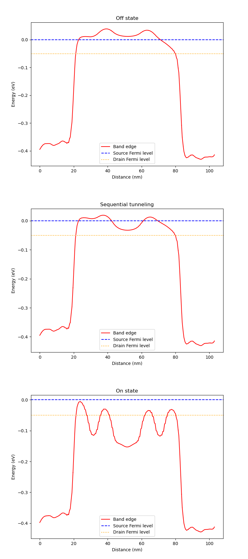
Fig. 4.7.1 Conduction band edge of the FD-SOI FET considered in this tutorial under three different regimes of operation.
Inspecting the contour plot of the LDOS shown below (specifically, the second plot, for the LDOS in the sequential-tunneling regime) the quantum dot appears to have at least one quasi-bound states at around \(-15~\textrm{meV}\). Since this quasi-bound state lies between the source and drain Fermi levels, electrons may tunnel between the source, this quasi-bound state, and the drain; this is transport in the sequential tunneling regime. It is also worth noting that due to the finite lifetime of this quasi-bound state, it does not have a precisely defined energy. This results in the quasi-bound state appearing as a “blob” in the LDOS contour plot. One may also notice signs of quantum interferences in the LDOS. This notably includes oscillations in the LDOS in the source and drain (which appear as vertical blue lines in the contour plot); these arise as a result of source-injected (drain-injected) electrons being reflected back to the source (drain) by the potential barrier at the source–channel (channel–drain) interface.
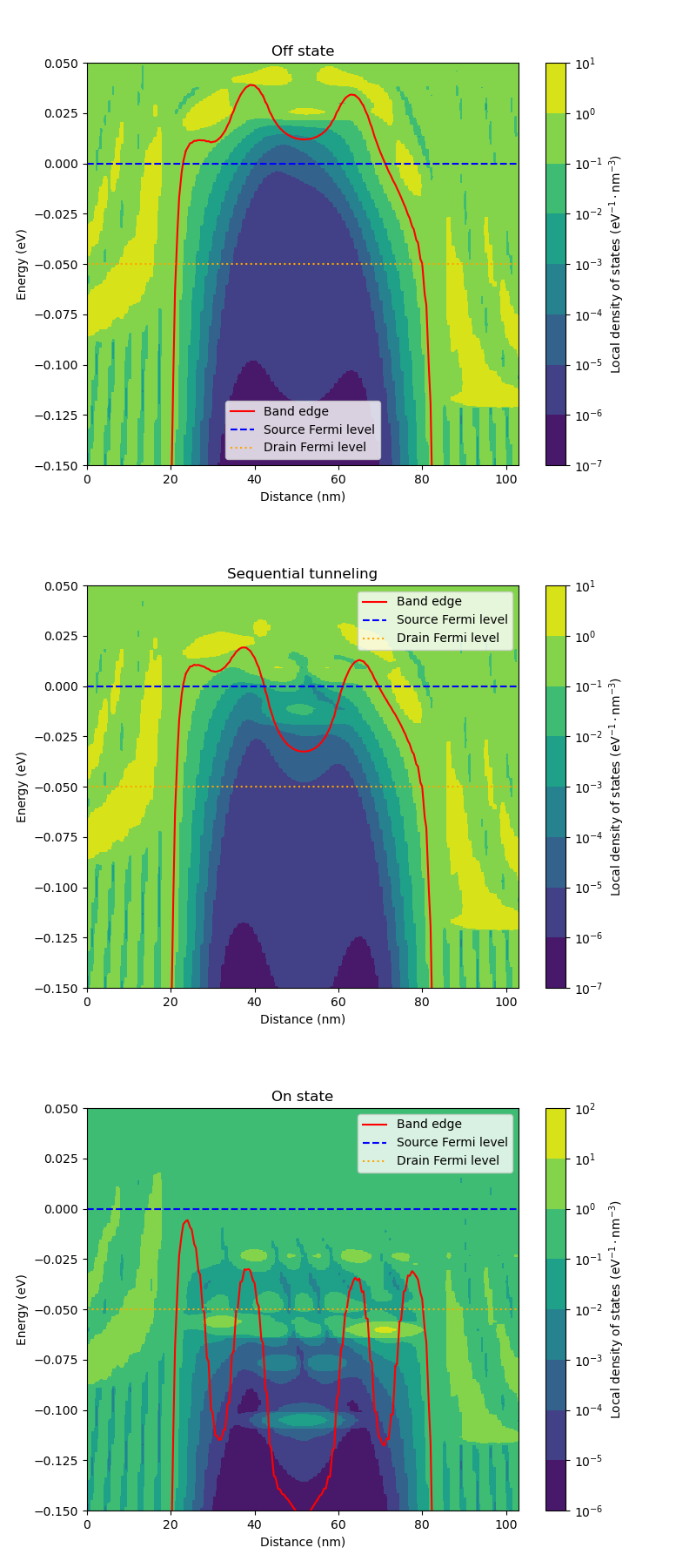
Fig. 4.7.2 Local density of states (LDOS) of the FD-SOI FET considered in this tutorial under three different regimes of operation.
The plots of the spectral current, which we show below, confirm the physical picture we have painted regarding transport in the sequential tunneling regime. Indeed, in this regime, the spectral current exhibits a sharp peak around \(-15~\textrm{meV}\), namely the energy of the quantum dot’s quasi-bound state. Moreover, in the off-state and on-state, the spectral current very sharply falls to zero above the source Fermi level due to the sub-Kelvin temperature assumed in this tutorial (see the Fermi–Dirac distributions appearing in Eq. (11.10)). Also note that the spectral current in the off state exhibits a peak at around \(-47~\textrm{meV}\), an energy at which the channel quantum dot appears to harbor a quasi-bound state.
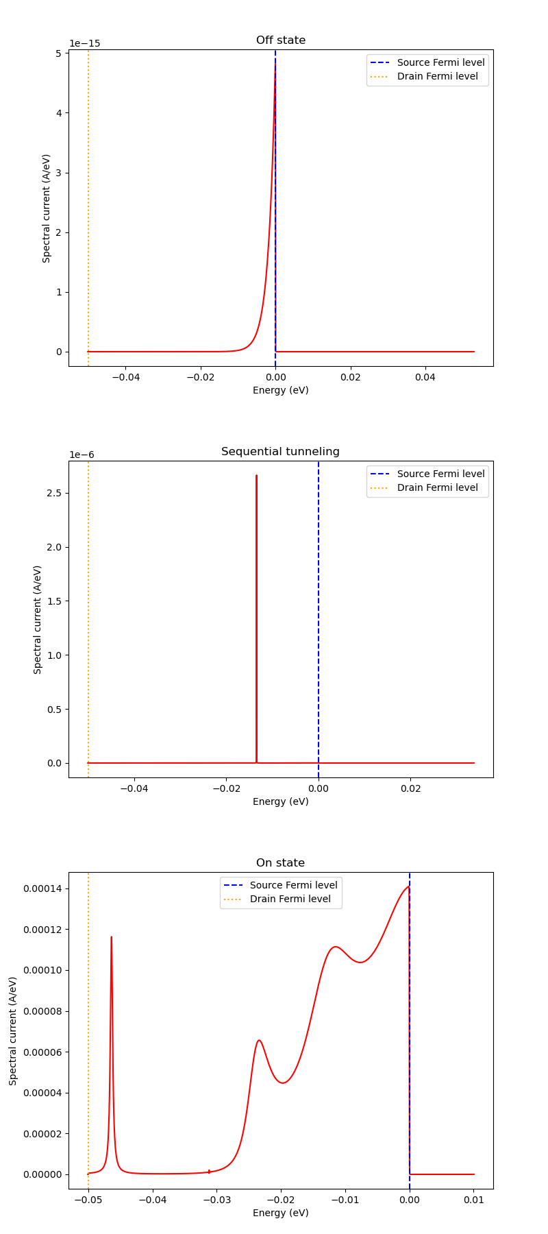
Fig. 4.7.3 Spectral current of the FD-SOI FET considered in this tutorial under three different regimes of operation.
It is also worth noting that the very sharp peak that the spectral current
exhibits in the sequential-tunneling regime can readily and efficiently be
resolved, without resorting to an extremely dense energy grid, thanks to the
adaptive integration algorithm internally used in the
get_current_adaptive
method.
Note
The QTCAD NEGF module ignores electron–electron (and hole–hole) interactions. As such, it cannot model transport in the Coulomb blockade regime. To model transport in the Coulomb blockade regime, users may explore the methods presented in Quantum transport—Master equation, Quantum transport—WKB approximation, and Quantum transport—Charge stability diagram of a double quantum dot.
Finally, outside of the for loop, we may print the values of the drain–source current in the three investigated regimes.
# Print values of current in three investigated regimes
for ii, regime in enumerate(regime_str):
   print("-".join(regime.split()) + " regime current: " + \
      str(current[ii]) + " A.")
This should result in the following.
Off-state regime current: 9.089833252296484e-18 A.
Sequential-tunneling regime current: 3.432416401909127e-11 A.
On-state regime current: 2.3787341502791564e-06 A.
Note that the sequential-tunneling regime current could be increased by reducing the size and/or height of the potential barriers between the source/drain and quantum dot. This could be achieved through tuning of the biases applied on the barrier gates and/or by reducing the lengths of the barrier gates. This current could also be increased by reducing the effective mass of charge carriers.
Finally, the total simulation time is automatically printed. On a machine with four logical cores, the simulation time was measured to be around one hour.
Exiting QTCAD script.
Total simulation time: 3888.648710565176 s
Note that the simulation time may exhibit significant variability from one machine to another.
4.8. Full code
__copyright__ = "Copyright 2022-2026, Nanoacademic Technologies Inc."

import pathlib
from os import cpu_count
import numpy as np
from qtcad.device import constants as ct
from qtcad.device.mesh3d import Mesh, SubMesh
from qtcad.device import materials as mt
from qtcad.device import Device, SubDevice
from qtcad.transport.negf_poisson import Solver, SolverParams

# Set up paths
script_dir = pathlib.Path(__file__).parent.resolve()
path_mesh = script_dir / "meshes"
path_out = script_dir / "output"

# Load the mesh
scaling = 1e-9
mesh = Mesh(scaling, str(path_mesh / "fdsoi_negf.msh"))

# Define the device object
d = Device(mesh, conf_carriers="e")
d.set_temperature(0.1)

# Create the regions
ndoping = 2e20 * 1e6
d.new_region("top_ox", mt.SiO2_ideal)
d.new_region("source", mt.Si, ndoping=ndoping)
d.new_region("channel", mt.Si)
d.new_region("drain", mt.Si, ndoping=ndoping)
d.new_region("side_bot_ox", mt.SiO2_ideal)

# Set up boundary condition for back gate
back_gate_bias = -0.2
doping_back_gate = 1e15 * 1e6
binding_energy = 46 * 1e-3 * ct.e
d.new_frozen_bnd(
    "back_gate_bnd", back_gate_bias, mt.Si, doping_back_gate, "n", binding_energy
)

# Set boundary conditions for source and drain of FET for NEGF simulation
d.new_quantum_lead_bnd("source_bnd", essential=False)
d.new_quantum_lead_bnd("drain_bnd", essential=False)
Vds = 0.05  # drain-to-source voltage

# Restrict calculation of charge density on a subdevice
submesh = SubMesh(mesh, ["source", "channel", "drain"])
d_negf = SubDevice(d, submesh)

# NEGF-Poisson solver parameters
solver_params = SolverParams()
# Compute NEGF at different energy values in parallel
if cpu_count() >= 4:
    n_jobs = 4
else:
    n_jobs = 1
solver_params.n_jobs = n_jobs
mixing_param = [0.05, 0.05, 0.02]

# Define parameters pertaining to linecuts over which various quantities will
# be plotted
t_top_ox = 2 * scaling  # top oxide thickness
t_si = 3 * scaling  # silicon film thickness
begin = (0, np.amin(mesh.glob_nodes[:, 1]), -t_top_ox - t_si / 5)
end = (0, np.amax(mesh.glob_nodes[:, 1]), -t_top_ox - t_si / 5)
energies = np.linspace(-0.15 * ct.e, 0.05 * ct.e, 50)
show_figure = False  # whether plots are shown

# Define the voltages corresponding to off state, sequential tunneling regime,
# and on state, respectively
Ew = mt.Si.Eg / 2 + mt.Si.chi  # gate metal workfunction
barrier_gate_biases = np.array([0.7, 0.7, 1.7])
plunger_gate_biases = np.array([0.7, 0.76, 1.7])
current = np.zeros_like(barrier_gate_biases)  # drain-to-source current
regime_str = ["Off state", "Sequential tunneling", "On state"]

for ii, barrier_gate_bias in enumerate(barrier_gate_biases):
    # Set the boundary conditions for the top gates
    d.new_gate_bnd("barrier_gate_1_bnd", barrier_gate_bias, Ew)
    d.new_gate_bnd("plunger_gate_bnd", plunger_gate_biases[ii], Ew)
    d.new_gate_bnd("barrier_gate_2_bnd", barrier_gate_bias, Ew)

    # Set up NEGF-Poisson solver, and solve
    solver_params.mixing_param = mixing_param[ii]
    solver = Solver(d=d, d_negf=d_negf, Vds=Vds, solver_params=solver_params)
    solver.solve()

    # Plot and save various quantities of interest
    ii_str = "_" + str(ii)
    title = regime_str[ii]  # title of the plots
    # Conduction band edge
    path_band = str(path_out / ("band" + ii_str + ".png"))
    solver.plot_band_edge(
        begin=begin, end=end, title=title, show_figure=show_figure, path=path_band
    )
    # Local density of states
    path_ldos = str(path_out / ("ldos" + ii_str + ".png"))
    solver.plot_ldos(
        begin=begin,
        end=end,
        energies=energies,
        title=title,
        show_figure=show_figure,
        path=path_ldos,
    )
    # Spectral current (and current)
    path_spectral_current = str(path_out / ("spectral_current" + ii_str + ".png"))
    current[ii] = solver.get_current_adaptive(
        log_scale=False,
        title=title,
        show_figure=show_figure,
        path=path_spectral_current,
    )

# Print values of current in three investigated regimes
for ii, regime in enumerate(regime_str):
    print("-".join(regime.split()) + " regime current: " + str(current[ii]) + " A.")