15. A double quantum dot device in a fully-depleted silicon-on-insulator transistor
15.1. Requirements
15.1.1. Software components
QTCAD®
Gmsh
15.1.2. Geometry file
qtcad/examples/tutorials/meshes/dqdfdsoi.geo
15.1.3. Python script
qtcad/examples/tutorials/helper/double_dot_fdsoi.py
15.2. Briefing
In this tutorial, we will define a function that produces a
Device object for a double quantum dot
in a generic fully-depleted silicon-on-insulator (FD-SOI) structure.
This function will be used in several subsequent tutorials in which various
physical phenomena will be studied under this geometry.
These tutorials are:
Quantum transport—Charge stability diagram of a double quantum dot
Tunnel coupling in a double quantum dot in FD-SOI—Part 1: Plunger gate tuning
Tunnel coupling in a double quantum dot in FD-SOI—Part 2: Tuning the barrier gate
Exchange coupling in a double quantum dot in FD-SOI—Part 1: Perturbation theory
Exchange coupling in a double quantum dot in FD-SOI—Part 2: Exact diagonalization
15.3. Device geometry
The device considered here is illustrated below.
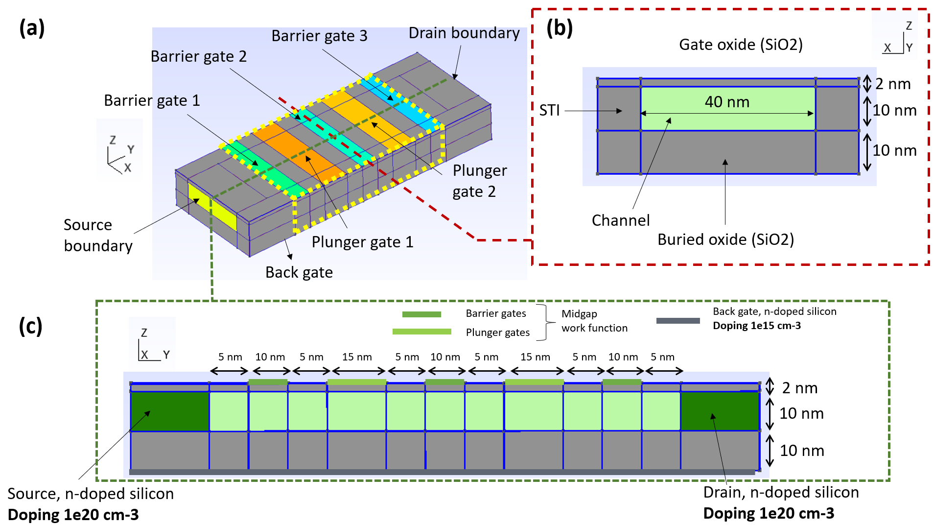
Fig. 15.3.1 Fully-depleted silicon-on-insulator (FD-SOI) structure hosting a gated double quantum dot. (a) Three-dimensional view of the structure, with colored surfaces indicating named boundaries. The gray color indicates regions where the material is silicon dioxide, and for which simulation domain boundaries obey default (natural) boundary conditions. The dotted yellow lines delineate the quantum dot region. (b) Slice across the channel. (c) Slice along the channel. Regions colored with the pale shade of green are intrinsic silicon, while the darker green regions are strongly n-doped silicon.
This device contains three layers.
The first layer consists of silicon dioxide, on which metallic control gates for the dots are deposited. These contacts are modeled by gate boundary conditions. For full double dot control, we use three “barrier gates” and two “plunger gates”. While barrier gates enable to control tunneling between the source, dot 1, dot 2, and the drain, the plunger gates control the detuning of the dot levels and their positions in energy space relative to the Fermi levels of the source and drain.
The second layer contains the silicon channel and the oxide that surrounds it. In Fig. 15.3.1 (b), the oxide in this layer is labeled by the STI acronym (which stands for “shallow trench isolation”). Ohmic boundary conditions are implemented on the two surfaces at the intersections of the source/drain volumes with the simulation domain boundaries. As illustrated in Fig. 15.3.1 (c), while the channel consists of intrinsic silicon, the source and drain are made of strongly n-doped silicon.
The third layer consists of a silicon dioxide sheet called the buried oxide. In the current context, the buried oxide will help achieve quantum confinement of electrons along the \(z\) direction. A boundary condition is applied to the entire surface at the bottom of the buried oxide to model body biasing through the back gate.
For strong doping above the critical Mott concentration, essentially all dopants are ionized in the deep cryogenic regime [Gru10, Kan20, PS12]. Therefore, in the source and drain, we use the default complete ionization model and usual Ohmic boundary conditions. By contrast, when doping is much weaker than the critical Mott concentration, essentially all donors are frozen (none are ionized) and the Fermi level is pinned halfway between the conduction band edge and the donor level. Assuming that the substrate below the buried oxide is weakly doped, we will therefore model the interface between the buried oxide and the substrate using a frozen boundary condition.
15.4. Header
We start by importing the necessary packages.
from qtcad.device import constants as ct
from qtcad.device import materials as mt
from qtcad.device import Device
15.5. Setting up the function that produces the device
In this tutorial, we create a function called get_double_dot_fdsoi that
outputs a Device object corresponding
to the double-dot FD-SOI structure.
The function takes as input the
Mesh object over which the device is
defined, and the potentials applied at each of the boundaries introduced above.
def get_double_dot_fdsoi(mesh, back_gate_bias, barrier_gate_1_bias,
   plunger_gate_1_bias, barrier_gate_2_bias, plunger_gate_2_bias,
   barrier_gate_3_bias):
   """Produce a Device object for a double quantum dot in a Fully-Depleted
   Silicon-On-Insulator (FD-SOI) transistor.

   Args:
      mesh (Mesh): The mesh over which the device is defined.
      back_gate_bias (float): The potential applied at the back gate.
      barrier_gate_1_bias (float): The potential applied at the first
         barrier gate.
      plunger_gate_1_bias (float): The potential applied at the first
         plunger gate.
      barrier_gate_2_bias (float): The potential applied at the second
         barrier gate.
      plunger_gate_2_bias (float): The potential applied at the second
         plunger gate.
      barrier_gate_3_bias (float): The potential applied at the third
         barrier gate.

   Returns:
      Device: The Device object for the double quantum dot structure.

   """

   # Define the device object
   dvc = Device(mesh, conf_carriers='e')
   dvc.set_temperature(0.1)

   # Create the regions
   dvc.new_region("oxide", mt.SiO2)
   dvc.new_region("oxide_dot", mt.SiO2)
   dvc.new_region("gate_oxide", mt.HfO2)
   dvc.new_region("gate_oxide_dot", mt.HfO2)
   dvc.new_region("buried_oxide", mt.SiO2)
   dvc.new_region("buried_oxide_dot", mt.SiO2)
   dvc.new_region("channel", mt.Si)
   dvc.new_region("channel_dot", mt.Si)
   dvc.new_region("source", mt.Si, ndoping=1e20*1e6)
   dvc.new_region("drain", mt.Si, ndoping=1e20*1e6)

   # Set up boundary conditions
   Ew = mt.Si.Eg/2 + mt.Si.chi # Midgap
   dvc.new_gate_bnd("barrier_gate_1_bnd", barrier_gate_1_bias, Ew)
   dvc.new_gate_bnd("plunger_gate_1_bnd", plunger_gate_1_bias, Ew)
   dvc.new_gate_bnd("barrier_gate_2_bnd", barrier_gate_2_bias, Ew)
   dvc.new_gate_bnd("plunger_gate_2_bnd", plunger_gate_2_bias, Ew)
   dvc.new_gate_bnd("barrier_gate_3_bnd", barrier_gate_3_bias, Ew)
   dvc.new_ohmic_bnd("source_bnd")
   dvc.new_ohmic_bnd("drain_bnd")
   dvc.new_frozen_bnd("back_gate_bnd", back_gate_bias, mt.Si, 1e15*1e6,
      "n", 46*1e-3*ct.e)

   # Create the double quantum dot region
   dot_region_list = ["oxide_dot", "gate_oxide_dot", "buried_oxide_dot", "channel_dot"]
   dvc.set_dot_region(dot_region_list)

   return dvc
Here, we create the device from the mesh, specify that confined carriers are electrons, and set the temperature to \(100~\mathrm{mK}\). We define the materials and boundary conditions, and define the dot region in which we expect the double quantum dot to be formed. As explained in earlier tutorials, classical charge is set to zero in this region. Here we choose the dot region to correspond to the volumes delineated by the dotted yellow lines in Fig. 15.3.1 (a).
In addition, we set a gate bias configuration from the arguments of the function for the back gate, plunger gates, and barrier gates. For the plunger gate and barrier gate boundaries, we use a Gate boundary condition with a work function that corresponds to midgap conditions, i.e., the Fermi level of the contact is aligned with the Fermi level of intrinsic silicon at zero temperature. In addition, for the back gate, we use the Frozen boundary condition, which is appropriate for Ohmic contacts with weakly doped semiconductors at cryogenic temperature. Here, we assume that the semiconductor below the buried oxide (which is in contact with the back gate) is n-doped silicon with a dopant concentration of \(10^{15}\;\mathrm{cm}^{-3}\). In addition, we use a dopant ionization energy of 46 \(\mathrm{meV}\), which is appropriate for phosphorus donors.
15.6. Full code
__copyright__ = "Copyright 2022-2026, Nanoacademic Technologies Inc."

from qtcad.device import constants as ct
from qtcad.device import materials as mt
from qtcad.device import Device


def get_double_dot_fdsoi(
    mesh,
    back_gate_bias,
    barrier_gate_1_bias,
    plunger_gate_1_bias,
    barrier_gate_2_bias,
    plunger_gate_2_bias,
    barrier_gate_3_bias,
):
    """Produce a Device object for a double quantum dot in a Fully-Depleted
    Silicon-On-Insulator (FD-SOI) transistor.

    Args:
       mesh (Mesh): The mesh over which the device is defined.
       back_gate_bias (float): The potential applied at the back gate.
       barrier_gate_1_bias (float): The potential applied at the first
          barrier gate.
       plunger_gate_1_bias (float): The potential applied at the first
          plunger gate.
       barrier_gate_2_bias (float): The potential applied at the second
          barrier gate.
       plunger_gate_2_bias (float): The potential applied at the second
          plunger gate.
       barrier_gate_3_bias (float): The potential applied at the third
          barrier gate.

    Returns:
       Device: The Device object for the double quantum dot structure.

    """

    # Define the device object
    dvc = Device(mesh, conf_carriers="e")
    dvc.set_temperature(0.1)

    # Create the regions
    dvc.new_region("oxide", mt.SiO2)
    dvc.new_region("oxide_dot", mt.SiO2)
    dvc.new_region("gate_oxide", mt.HfO2)
    dvc.new_region("gate_oxide_dot", mt.HfO2)
    dvc.new_region("buried_oxide", mt.SiO2)
    dvc.new_region("buried_oxide_dot", mt.SiO2)
    dvc.new_region("channel", mt.Si)
    dvc.new_region("channel_dot", mt.Si)
    dvc.new_region("source", mt.Si, ndoping=1e20 * 1e6)
    dvc.new_region("drain", mt.Si, ndoping=1e20 * 1e6)

    # Set up boundary conditions
    Ew = mt.Si.Eg / 2 + mt.Si.chi  # Midgap
    dvc.new_gate_bnd("barrier_gate_1_bnd", barrier_gate_1_bias, Ew)
    dvc.new_gate_bnd("plunger_gate_1_bnd", plunger_gate_1_bias, Ew)
    dvc.new_gate_bnd("barrier_gate_2_bnd", barrier_gate_2_bias, Ew)
    dvc.new_gate_bnd("plunger_gate_2_bnd", plunger_gate_2_bias, Ew)
    dvc.new_gate_bnd("barrier_gate_3_bnd", barrier_gate_3_bias, Ew)
    dvc.new_ohmic_bnd("source_bnd")
    dvc.new_ohmic_bnd("drain_bnd")
    dvc.new_frozen_bnd(
        "back_gate_bnd", back_gate_bias, mt.Si, 1e15 * 1e6, "n", 46 * 1e-3 * ct.e
    )

    # Create the double quantum dot region
    dot_region_list = ["oxide_dot", "gate_oxide_dot", "buried_oxide_dot", "channel_dot"]
    dvc.set_dot_region(dot_region_list)

    return dvc