8. Self-consistent Schrödinger–Poisson simulation of a MOS capacitor
8.1. Requirements
8.1.1. Software components
QTCAD
Gmsh
8.1.2. Geometry file
qtcad/examples/tutorials/meshes/moscap.geo
8.1.3. Python script
qtcad/examples/tutorials/moscap.py
8.1.4. References
8.2. Briefing
In this tutorial, we explain how to perform a self-consistent Schrödinger–Poisson calculation of a 1D metal–oxide–semiconductor (MOS) capacitor structure. The same approach would also work for 2D and 3D meshes; this 1D structure is simply chosen for its simplicity.
The full code may be found at the bottom of this page,
or in qtcad/examples/tutorials/moscap.py.

Fig. 8.2.1 The metal–oxide–semiconductor (MOS) capacitor being simulated here. The metal acts as a gate boundary condition, and is not simulated. The origin of the \(x\) axis is at the metal–oxide interface. Because of translational invariance along \(y\) and \(z\), the problem reduces to a 1D problem.
8.3. Setting up the device and solving the electrostatic problem
8.3.1. Header
A header is first written to import relevant modules from the QTCAD Device simulator, and from standard Python libraries.
import numpy as np
from matplotlib import pyplot as plt
from pathlib import Path

from qtcad.device import analysis as an
from qtcad.device import materials as mt
from qtcad.device import constants as ct
from qtcad.device import Device, Mesh1D
from qtcad.device.schrodinger_poisson import Solver, SolverParams
from qtcad.device.poisson import SolverParams as PoissonSolverParams
from qtcad.device.schrodinger import SolverParams as SchrodingerSolverParams
These modules are the same as in previous tutorials, except for the
schrodinger_poisson module,
which defines the self-consistent Schrödinger–Poisson
Solver Solver class.
In addition, we have imported SolverParams classes of the
schrodinger_poisson,
poisson, and
schrodinger modules.
8.3.2. Input parameters
We first introduce useful paths.
# Relevant paths
path = Path(__file__).parent.resolve()
path_mesh = path / "meshes" / "moscap.msh"
path_cond_band_edge_schred = path / "data" / "cond_band_edge.txt"
path_ground_schred = path / "data" / "ground.txt"
path_first_excited_schred = path / "data" / "first_excited.txt"
The first line defines the path to the script being run. The next lines define paths to simulation results obtained using the free open-source software SCHRED, which is a specialized 1D Schrödinger–Poisson solver for specific 1D semiconductor structures, such as MOS capacitors. We will use these simulation results to compare with QTCAD.
After defining the paths, we define some important device parameters.
# Some device parameters
temperature = 100
gate_phi = 1.3
doping = 1e18*1e6
work_function = mt.Si.chi+mt.Si.Eg/2    # Midgap
The first parameter is the device temperature, assumed to be homogeneous. We choose \(100 \textrm{ K}\) because this is the lowest temperature at which SCHRED converges for the structure that we will simulate. The second parameter is the applied potential at the metallic gate. The third parameter is the semiconductor doping concentration in \(\mathrm m^{-3}\). The last parameter is the metallic gate work function; here we choose midgap conditions.
We will choose the semiconductor to be silicon.
As discussed in Multivalley effective-mass theory solver and as illustrated in Fig. 5.1 (b), silicon has six equivalent conduction band minima, called valleys; the equipotential surfaces for these minima are elongated ellipsoids aligned with the Cartesian directions. For each valley, there are two smaller equal (transverse) effective masses \(m_t\), and one larger (longitudinal) effective mass \(m_l\) along the Cartesian direction.
Here, we will see that the MOS capacitor will yield a triangular confinement potential along \(x\).
Because effective mass along the \(x\) direction for the \(\pm \mathbf{y}\) and \(\pm \mathbf{z}\) valleys is the smaller (transverse) effective mass \(m_t\), the orbital ground state for these valleys will be higher than for the \(\pm \mathbf{x}\) valleys, for which effective mass along \(x\) is the larger (longitudinal) effective mass. This is simply because energy levels under quantum confinement decrease as effective mass is increased (e.g. in the particle-in-a-box problem). Consequently, under sufficiently strong confinement along \(x\), the \(\pm \mathbf{y}\) and \(\pm \mathbf{z}\) valleys may be neglected in a first approximation, since their minima lie much higher in energy than the \(\pm \mathbf{x}\) valleys. We are thus left with a total electron degeneracy factor \(g_{q,e}=4\): 2 for spin, and 2 for the \(\pm \mathbf{x}\) valleys, which is the default value for silicon in QTCAD (see the Schrödinger–Poisson theory section).
By default, in QTCAD, the inverse effective mass tensor of silicon is
i.e. the longitudinal effective mass is aligned with the \(z\) axis.
Following the above discussion on valleys, we must thus rotate this inverse effective mass tensor to correspond to the \(\pm\mathbf{\hat x}\) valleys that are relevant here.
This is done with:
# Rotate the effective mass tensor so that the longitudinal effectice mass
# aligns with the x axis
inv_mass_tensor = mt.Si.Me_inv.copy()
inv_mass_tensor[0,0] = mt.Si.Me_inv[2,2]
inv_mass_tensor[2,2] = mt.Si.Me_inv[0,0]
mt.Si.set_param("Me_inv", inv_mass_tensor)
Note
Instead of rotating the effective mass tensor, one could also specify the
translationally invariant directions of the system to be the
\(x\) and \(y\) directions using the
ti_directions
solver parameter of the Schrödinger
solver.
In this specific example we could have used
schrodinger_params.ti_directions = ["x", "y"] below.
By default, the Schrödinger solver assumes that the translationally invariant
directions are those transverse to the mesh direction.
In this example, the mesh is along the \(x\) direction, so the
translationally invariant directions are the \(y\) and \(z\)
directions.
8.3.3. Defining the mesh and the device
As usual the mesh is defined by loading the mesh file produced by Gmsh and setting units of length. The device is then instantiated on the resulting mesh
# First load the mesh and create the device
scale = 1e-9
mesh = Mesh1D(scale, path_mesh)
dvc = Device(mesh, conf_carriers="e")
We then set the device temperature, and set up confined carriers to be electrons. In addition, we will use the incomplete dopant ionization model.
# Set temperature to 100 K
dvc.set_temperature(temperature)

# Set up confined carriers to be electrons (this is the default value)
# and ionization model to incomplete
dvc.ionization = "incomplete"
The next step is to define device regions. Because SCHRED does not model penetration of the wave function into the oxide, we will use the ideal version of the \(\mathrm {SiO}_2\) material, which forces the wave function to be zero in the oxide.
# Define device regions
dvc.new_region("oxide", mt.SiO2_ideal)
dvc.new_region("semi", mt.Si, pdoping = doping)
Finally, we set the boundary conditions for the metallic gate on the left, and for the rightmost edge of the simulation domain. On the right, we use an Ohmic boundary condition, which assumes that the semiconductor is at a charge-neutral equilibrium with its environment at this point.
# Define boundary conditions
dvc.new_gate_bnd("gate_bnd", gate_phi, work_function)
dvc.new_ohmic_bnd("ohmic_bnd")
8.3.4. Setting up and running the Schrödinger–Poisson solver
We will create and configure three
SolverParams objects.
This is because we want to configure not only the self-consistent
Schrödinger–Poisson solver, but also the individual Poisson and Schrödinger
solvers that are involved in the self-consistent loops.
The sp_params object parametrizes the Schrödinger-Poisson solver and has
attributes poisson_solver_params and schrod_solver_params which
parametrize the internal Poisson and Schrödinger solvers, respectively.
This is done with:
# Set up solver parameters
sp_params = SolverParams()
sp_params.tol = 1e-5
sp_params.maxiter = 200

poisson_params = PoissonSolverParams()
poisson_params.tol = 1e-5

schrodinger_params = SchrodingerSolverParams()
schrodinger_params.num_states = 8

sp_params.poisson_solver_params = poisson_params
sp_params.schrod_solver_params = schrodinger_params
In the first block of code, we set the tolerance on electric potential to \(10^{-5}\textrm{ V}\) for the Schrödinger–Poisson solver, and set the maximum number of self-consistent iterations to \(200\).
In the second block of code, we set the tolerance on electric potential to \(10^{-5}\textrm { V}\) also for the Poisson solver.
Finally, in the last block of code, we choose to keep only eight orbital energy levels in the simulation. Here, this choice is rather arbitrary and used to illustrate how to set up solver parameters. However, it is important to check that the simulation results do not depend on the number of levels. At sufficiently high temperatures compared with level spacing, many levels may become populated, and more levels should be kept.
Once the solver parameters are configured, we instantiate the Schrödinger–Poisson solver and run it with:
# Instantiate the Schrodinger-Poisson solver
slv = Solver(dvc, solver_params=sp_params)

# Solve Schrodinger-Poisson
slv.solve()
8.4. Visualizing results
8.4.1. Band diagram
We plot the band diagram of the device with:
# Plot the band diagram
an.plot_bands(dvc)
which results in
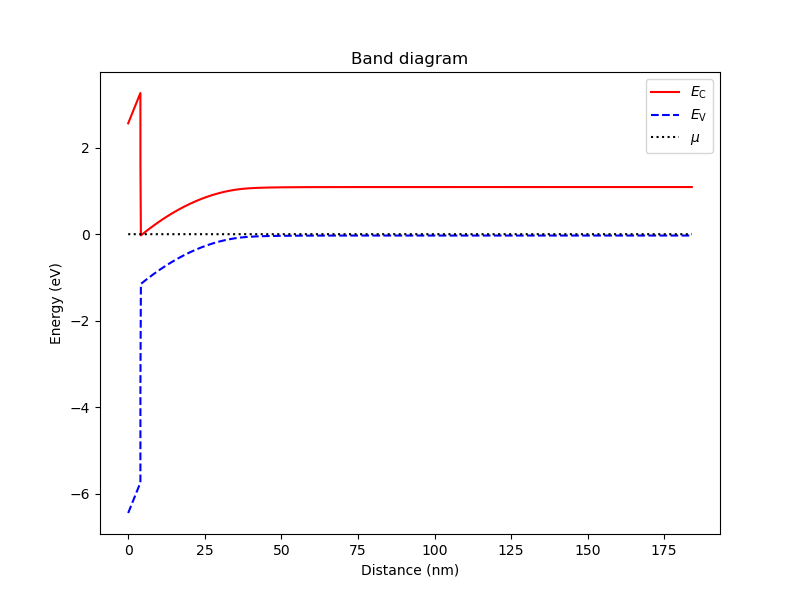
Fig. 8.4.1 Band diagram for the MOS capacitor.
8.4.2. Comparison with SCHRED
Following [GNM+13], we then compare our simulation outputs to results obtained with SCHRED.
To do so, we will plot our results with PyPlot. We must first define all our simulation outputs over global nodes ordered with increasing \(x\). This is done with:
# Sort the nodes
sort_indices = np.argsort(mesh.glob_nodes[:,0])
x = mesh.glob_nodes[sort_indices,0]/1e-9
cond_band_edge = mesh.toglobal(dvc.cond_band_edge()/ct.e)
ground = dvc.eigenfunctions[sort_indices,0]
first_excited = dvc.eigenfunctions[sort_indices,1]
This is important because:
There is no guarantee that Gmsh sorts nodes in increasing \(x\) order.
The conduction band edge is defined over local nodes rather than global nodes. In other words, a value is given for each local node of each 1D element, resulting in a 2D array; PyPlot rather requires 1D arrays for both the \(x\) coordinate and the quantity being plotted.
After this, we load SCHRED simulation results.
# Load results from SCHRED
x_cond_band_edge_schred, cond_band_edge_schred\
    = np.loadtxt(path_cond_band_edge_schred).T
x_eigenfunctions_schred, ground_schred = np.loadtxt(path_ground_schred).T
x_eigenfunctions_schred, first_excited_schred\
    = np.loadtxt(path_first_excited_schred).T
Above, we loaded simulation results for the conduction band edge, and for the ground and first excited orbital eigenstates.
We first compare conduction band edges with:
# Compare conduction band edges
fig = plt.figure()
ax = fig.add_subplot(1,1,1)
ax.set_xlabel("$x$ (nm)")
ax.set_ylabel("$E_C$ (eV)")
ax.plot(x_cond_band_edge_schred, cond_band_edge_schred, ".k", label="SCHRED")
ax.plot(x, cond_band_edge, "-r", label="QTCAD")
ax.set_xlim(0,50)
ax.legend()
plt.show()
which results in:
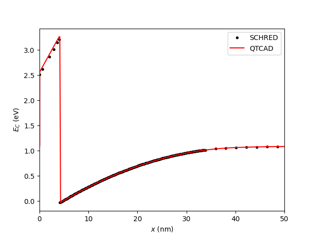
Fig. 8.4.2 MOS capacitor: comparison of the conduction band edge calculated with QTCAD and SCHRED.
Finally, we compare envelope functions with:
# Compare envelope functions
fig = plt.figure()
ax = fig.add_subplot(1,1,1)
ax.set_xlabel("$x$ (nm)")
ax.set_ylabel("Ground state (arb. units)")
ax.plot(x_eigenfunctions_schred, ground_schred, ".k",
    label="Ground state (SCHRED)")
ax.plot(x_eigenfunctions_schred, first_excited_schred, "^g",
    label="First excited state (SCHRED)")
ax.plot(x, np.abs(ground), "-r", label="Ground state (QTCAD)")
sign = np.sign(first_excited[np.isclose(x,10.)])[0] # Pick phase for wf>0 at x=10
ax.plot(x, first_excited*sign, "--b", label="First excited state (QTCAD)")
ax.set_xlim(0,20)
ax.legend()
plt.show()
which results in:
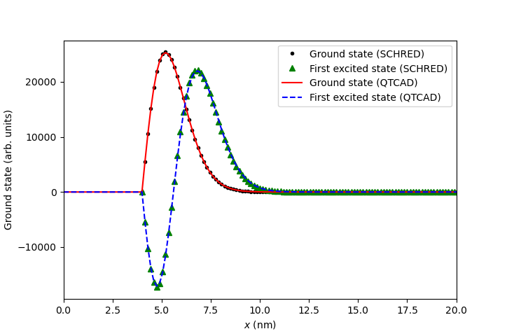
Fig. 8.4.3 MOS capacitor: comparison of the conduction band edge calculated with QTCAD and SCHRED.
In both cases, agreement is excellent.
8.5. Full code
__copyright__ = "Copyright 2022-2026, Nanoacademic Technologies Inc."

import numpy as np
from matplotlib import pyplot as plt
from pathlib import Path
from qtcad.device import analysis as an
from qtcad.device import materials as mt
from qtcad.device import constants as ct
from qtcad.device import Device, Mesh1D
from qtcad.device.schrodinger_poisson import Solver, SolverParams
from qtcad.device.poisson import SolverParams as PoissonSolverParams
from qtcad.device.schrodinger import SolverParams as SchrodingerSolverParams

# Relevant paths
path = Path(__file__).parent.resolve()
path_mesh = path / "meshes" / "moscap.msh"
path_cond_band_edge_schred = path / "data" / "cond_band_edge.txt"
path_ground_schred = path / "data" / "ground.txt"
path_first_excited_schred = path / "data" / "first_excited.txt"

# Some device parameters
temperature = 100
gate_phi = 1.3
doping = 1e18 * 1e6
work_function = mt.Si.chi + mt.Si.Eg / 2  # Midgap

# Rotate the effective mass tensor so that the longitudinal effectice mass
# aligns with the x axis
inv_mass_tensor = mt.Si.Me_inv.copy()
inv_mass_tensor[0, 0] = mt.Si.Me_inv[2, 2]
inv_mass_tensor[2, 2] = mt.Si.Me_inv[0, 0]
mt.Si.set_param("Me_inv", inv_mass_tensor)

# First load the mesh and create the device
scale = 1e-9
mesh = Mesh1D(scale, path_mesh)
dvc = Device(mesh, conf_carriers="e")

# Set temperature to 100 K
dvc.set_temperature(temperature)

# Set up confined carriers to be electrons (this is the default value)
# and ionization model to incomplete
dvc.ionization = "incomplete"

# Define device regions
dvc.new_region("oxide", mt.SiO2_ideal)
dvc.new_region("semi", mt.Si, pdoping=doping)

# Define boundary conditions
dvc.new_gate_bnd("gate_bnd", gate_phi, work_function)
dvc.new_ohmic_bnd("ohmic_bnd")

# Set up solver parameters
sp_params = SolverParams()
sp_params.tol = 1e-5
sp_params.maxiter = 200

poisson_params = PoissonSolverParams()
poisson_params.tol = 1e-5

schrodinger_params = SchrodingerSolverParams()
schrodinger_params.num_states = 8

sp_params.poisson_solver_params = poisson_params
sp_params.schrod_solver_params = schrodinger_params

# Instantiate the Schrodinger-Poisson solver
slv = Solver(dvc, solver_params=sp_params)

# Solve Schrodinger-Poisson
slv.solve()


# Plot the band diagram
an.plot_bands(dvc)

# Sort the nodes
sort_indices = np.argsort(mesh.glob_nodes[:, 0])
x = mesh.glob_nodes[sort_indices, 0] / 1e-9
cond_band_edge = mesh.toglobal(dvc.cond_band_edge() / ct.e)
ground = dvc.eigenfunctions[sort_indices, 0]
first_excited = dvc.eigenfunctions[sort_indices, 1]

# Load results from SCHRED
x_cond_band_edge_schred, cond_band_edge_schred = np.loadtxt(
    path_cond_band_edge_schred
).T
x_eigenfunctions_schred, ground_schred = np.loadtxt(path_ground_schred).T
x_eigenfunctions_schred, first_excited_schred = np.loadtxt(path_first_excited_schred).T

# Compare conduction band edges
fig = plt.figure()
ax = fig.add_subplot(1, 1, 1)
ax.set_xlabel("$x$ (nm)")
ax.set_ylabel("$E_C$ (eV)")
ax.plot(x_cond_band_edge_schred, cond_band_edge_schred, ".k", label="SCHRED")
ax.plot(x, cond_band_edge, "-r", label="QTCAD")
ax.set_xlim(0, 50)
ax.legend()
plt.show()

# Compare envelope functions
fig = plt.figure()
ax = fig.add_subplot(1, 1, 1)
ax.set_xlabel("$x$ (nm)")
ax.set_ylabel("Ground state (arb. units)")
ax.plot(x_eigenfunctions_schred, ground_schred, ".k", label="Ground state (SCHRED)")
ax.plot(
    x_eigenfunctions_schred,
    first_excited_schred,
    "^g",
    label="First excited state (SCHRED)",
)
ax.plot(x, np.abs(ground), "-r", label="Ground state (QTCAD)")
sign = np.sign(first_excited[np.isclose(x, 10.0)])[0]  # Pick phase for wf>0 at x=10
ax.plot(x, first_excited * sign, "--b", label="First excited state (QTCAD)")
ax.set_xlim(0, 20)
ax.legend()
plt.show()