3. Poisson solver with background charges
3.1. Requirements
3.1.1. Software components
QTCAD
Gmsh
3.1.2. Geometry file
qtcad/examples/tutorials/meshes/nanowire_background_charges.geo
3.1.3. Python script
qtcad/examples/tutorials/background_charges.py
3.1.4. References
3.2. Briefing
In this tutorial, we explain how to solve Poisson’s equation in the presence of user-defined background charges.
We consider the same nanowire as in the previous two tutorials, namely, Poisson and Schrödinger simulation of a nanowire quantum dot and Poisson solver with adaptive meshing. We again consider cryogenic temperature, at which convergence is challenging, and thus use adaptive meshing exactly as in the previous tutorial.
However, compared with previous tutorials, we consider the effect of parasitic background charges that are manually added in two ways.
1. We add a constant negative surface charge density at the interface between the channel and the surrounding oxide.
2. We add a constant Gaussian-shaped volume charge density distribution inside this same oxide, exactly halfway through the channel length.
The first background charge model may be used to model ensembles of charge traps that often form at interfaces between semiconductors and oxides. The second background charge model may be used to model an individual charge trap, for example at a dopant. Here, we use a Gaussian function for the volume charge density, but any other function of Cartesian coordinates \(x\), \(y\), and \(z\) may likewise be used.
3.3. Geometry file
As before, the initial mesh is generated from a
geometry file qtcad/examples/tutorials/meshes/nanowire_background_charges.geo
by running Gmsh with
gmsh nanowire_background_charges.geo
As in Poisson solver with adaptive meshing, this will produce both .msh and .geo_unrolled
files, as required by the adaptive-mesh Poisson solver for geometries
produced using the built-in Gmsh geometry kernel.
As will be seen below, an additional Gmsh physical surface is needed in comparison with the previous tutorials. This additional physical surface corresponds to the interface between the intrinisic silicon channel and the surrounding oxide, where we wish to introduce a background surface charge density. Thanks to the simple geometry of the nanowire device, it is straightforward to identify and label this surface directly within the Gmsh script. In more complicated cases, it may be easier to enter the Gmsh GUI, perform any clipping that may be required for the relevant elementary surfaces to become visible, and click on them to define the physical surface bearing the surface charge to be defined in QTCAD.
3.4. Setting up the device and the Poisson solver
3.4.1. Header and input parameters
The header and input parameters are almost the same as in the previous tutorial
import pathlib
import numpy as np
from copy import deepcopy
from matplotlib import pyplot as plt

from qtcad.device import constants as ct
from qtcad.device.mesh3d import Mesh
from qtcad.device import analysis
from qtcad.device import materials as mt
from qtcad.device import Device
from qtcad.device.poisson import Solver, SolverParams
The only difference is that we import the following additional standard Python packages:
pathlib,numpy,pyplot,
along with the deepcopy function of the copy package.
We next define geometry parameters exactly as in the previous tutorial.
# Define some device parameters
Vgs = 2.0                               # Gate-source bias
Ew = mt.Si.chi + mt.Si.Eg/2 # Metal work function
Ltot = 20e-9 # Device height in m
radius = 2.5e-9 # Device radius in m
The next step is to define parameters of the background charge densities.
# Background charge parameters
surf_charge_dnsty = -ct.e*5e17    # Surface charge density in C/m^2
vol_charge = -5*ct.e  # Total charge in background volume charge density in C
vol_charge_spread = 1e-9    # Standard deviation of Gaussian charge density in m
Finally, we define paths to the mesh and raw geometry files.
# Paths to mesh file and output files
script_dir = pathlib.Path(__file__).parent.resolve()
path_mesh = script_dir / "meshes" / "nanowire_background_charges.msh"
path_geo = script_dir / "meshes" / "nanowire_background_charges.geo_unrolled"
3.4.2. Loading the initial mesh and defining the device
We load the mesh and define the device exactly as in the previous tutorial.
# Load the mesh
scaling = 1e-9
mesh = Mesh(scaling, str(path_mesh))

# Create device and set temperature to 10 mK
dvc = Device(mesh, conf_carriers="e")
dvc.set_temperature(10e-3)

# Create regions first. The last added region takes priority for
# nodes that are shared by multiple regions.
# Make sure each nodes is assigned to a region, otherwise default
# (silicon) parameters are used
dvc.new_region('channel_ox',mt.SiO2)
dvc.new_region('source_ox',mt.SiO2)
dvc.new_region('drain_ox',mt.SiO2)
dvc.new_region('channel', mt.Si)
dvc.new_region('source', mt.Si, pdoping=5e20*1e6, ndoping=0)
dvc.new_region('drain', mt.Si, pdoping=5e20*1e6, ndoping=0)

# Then create boundaries
dvc.new_ohmic_bnd('source_bnd')
dvc.new_ohmic_bnd('drain_bnd')
dvc.new_gate_bnd('gate_bnd',Vgs,Ew)
However, here, we use deepcopy to create a copy of this initial device,
in which no background charge has been defined yet.
# Keep a copy of the device in which no background charge is used
dvc_no_charge = deepcopy(dvc)
This copy will be used later as a reference to analyze the impact of the background charges.
3.4.3. Setting up the background charge densities
We first add a (uniform) surface charge density at the interface between the
intrinisic channel and the surrounding oxide. This is done with the method
set_surf_charge_density
of the Device class.
# Add surface charge at interface between silicon channel and SiO2
dvc.set_surf_charge_density("interface", surf_charge_dnsty)
Here, the first argument is a string labeling the Gmsh physical surface corresponding to the interface, and the second argument is a float giving the value of the uniform surface charge density in \(\mathrm{C}/\mathrm{m}^2\).
In addition to this surface charge, we also define a background volume charge
density. This is done with the
set_vol_charge_density
method of the Device class. From the API
reference of this method, we see that there are two possible ways to set this
volume charge density: (i) a uniform value is chosen for a given region, (ii)
an arbitrary function of Cartesian coordinates \(x\), \(y\), and
\(z\) is given as input. Here, we use the latter approach. We first
define a function for the Gaussian charge distribution that we wish to use,
and then pass it as an argument to the
set_vol_charge_density
method.
# Create function for the volume charge density
# Take a Gaussian-shaped charge density in the SiO2 in proximity to the Si
# channel
x0 = 0; y0 = 2.0e-9; z0 = 10e-9
def gaussian(x, y, z):
   norm_factor = vol_charge/((2*np.pi)**(3/2.)*vol_charge_spread**3)
   numerator = (x-x0)**2+(y-y0)**2+(z-z0)**2
   denominator = 2*vol_charge_spread**2
   return norm_factor*np.exp(-numerator/denominator)

dvc.set_vol_charge_density(gaussian)
From this definition, we may easily show that the integral of the Gaussian
function over all real space is given by vol_charge, which we chose to be
equal to \(-5\mathrm e\) in the header of this script. In addition, we chose
the charge density to be quite concentrated, with a standard deviation of
\(1\;\mathrm{nm}\). This choice is arbitrary and was made to make the
effects of the background volume charge as visible as possible without yet
becoming dominant over the entire device. For realistic device modeling,
appropriate total charges and charge distribution functions should be chosen
in accordance with typical charge defects to be studied.
3.4.4. Setting up the adaptive-mesh Poisson solver
The next step is to set up the parameters of the adaptive-mesh Poisson solver. Here we proceed exactly as in the previous tutorial, except that we set the minimum number of nodes to 20,000 to ensure that the resolution of the final mesh is satisfactory.
# Configure the non-linear Poisson solver
params_poisson = SolverParams()
params_poisson.tol = 1e-5 # Convergence threshold (tolerance) for the error
params_poisson.initial_ref_factor = 0.1
params_poisson.final_ref_factor = 0.75
params_poisson.min_nodes = 20000
After defining Poisson solver parameters, we instantiate two Poisson solver objects: one for the full device including background charges, and another for the original device without background charges.
# Create an adaptive-mesh non-linear Poisson solver for each device
slv = Solver(dvc, solver_params=params_poisson, geo_file=path_geo)
slv_no_charge = Solver(dvc_no_charge, solver_params=params_poisson,
   geo_file=path_geo)
3.5. Solving Poisson’s equation and analyzing the results
We launch the Poisson simulations first without background charges, and then including background charges, with:
# Self-consistent solution for each device
print("="*80)
print("SOLVING NON-LINEAR POISSON WITHOUT BACKGROUND CHARGES")
print("="*80)
slv_no_charge.solve()

print("="*80)
print("SOLVING NON-LINEAR POISSON WITH BACKGROUND CHARGES")
print("="*80)
slv.solve()
After convergence of the two Poisson solvers, we consider the conduction band edge with and without background charges along two linecuts: a first linecut along the \(z\) axis (the symmetry axis of the cylinders defining the nanowire), and a second linecut parallel to the \(y\) axis (perpendicular to the nanowire symmetry axis) but exactly halfway through the channel. The linecuts are taken with
# Evaluate conduction band edge along linecuts to compare the two cases

## Linecut along symmetry axis of the nanowire
z, band_edge_z = analysis.linecut(dvc.mesh, dvc.cond_band_edge()/ct.e,
   (0,0,0), (0,0,Ltot))
z_no_charge, band_edge_z_no_charge = analysis.linecut(dvc_no_charge.mesh,
   dvc_no_charge.cond_band_edge()/ct.e, (0,0,0), (0,0,Ltot))

## Linecut along y axis
y, band_edge_y = analysis.linecut(dvc.mesh, dvc.cond_band_edge()/ct.e,
   (0,-radius,Ltot/2), (0,radius,Ltot/2))
y_no_charge, band_edge_y_no_charge = analysis.linecut(dvc_no_charge.mesh,
   dvc_no_charge.cond_band_edge()/ct.e, (0,-radius,Ltot/2), (0,radius,Ltot/2))
Note that the second linecut passes through the mode of the Gaussian distribution of the background volume charge.
We then produce plots of the linecuts with
# Produce plots of the linecuts
fig = plt.figure(figsize=(8,7))

ax1 = fig.add_subplot(2,1,1)
ax1.set_xlabel("$z$ (nm)")
ax1.set_ylabel("$E_C$ (eV)")
ax1.plot(z/1e-9, band_edge_z, "-b", label="With background charge")
ax1.plot(z_no_charge/1e-9, band_edge_z_no_charge, "-r",
   label="Without background charge")
ax1.legend()

ax2 = fig.add_subplot(2,1,2)
ax2.set_xlabel("$y$ (nm)")
ax2.set_ylabel("$E_C$ (eV)")
ax2.plot(y/1e-9, band_edge_y, "-b", label="With background charge")
ax2.plot(y_no_charge/1e-9, band_edge_y_no_charge, "-r",
   label="Without background charge")
ax2.legend()
plt.show()
This results in
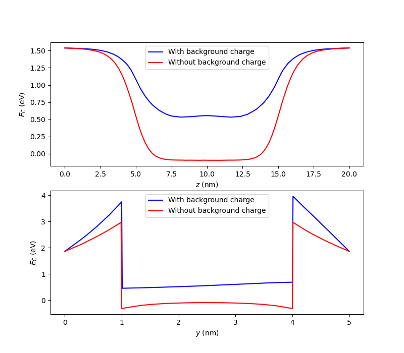
Fig. 3.5.1 Band diagram along (a) first linecut along \(z\), (b) second linecut along \(y\) halfway through the channel.
We see that the presence of both surface and volume negative background charges raises the conduction band edge of the channel, as may be expected intuitively. In particular, the localized defect modeled through the Gaussian-shaped volume charge density creates a small potential barrier which is visible in the middle of the linecut in subfigure (a). Similarly, this charge raises the conduction band edge in the neighboring oxide, as may be seen in subfigure (b). In addition, subfigure (b) shows that while without background charges, the derivative of the band edge is roughly constant across the interface between the channel and the oxide, this is clearly not the case anymore in the presence of background charges. Indeed, the negatively charged surface almost completely suppresses the triangular potential well that was formed in the channel near the interface with the oxide in the absence of background charges, while maintaining a strong potential gradient in the oxide consistent with electrons being repelled away from the interface.
Finally, we plot the charge density in the device that includes background charges over orthogonal slices.
# Plot charge density in device with background charges along slices
analysis.plot_slices(dvc.mesh, dvc.rho/ct.e/1e6, title="rho/e (cm^-3)")
This results in the following figure.
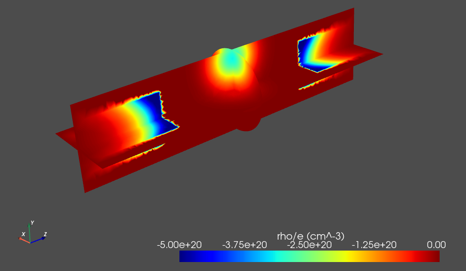
Fig. 3.5.2 Charge density on orthogonal slices of the nanowire geometry.
While the effect of surface charges is not clearly visible in this plot, we easily see a bright halo halfway through the channel that corresponds to the localized negative charge defect modeled using the Gaussian background volume charge density.
3.6. Full code
__copyright__ = "Copyright 2022-2026, Nanoacademic Technologies Inc."

import pathlib
import numpy as np
from copy import deepcopy
from matplotlib import pyplot as plt
from qtcad.device import constants as ct
from qtcad.device.mesh3d import Mesh
from qtcad.device import analysis
from qtcad.device import materials as mt
from qtcad.device import Device
from qtcad.device.poisson import Solver, SolverParams

# Define some device parameters
Vgs = 2.0  # Gate-source bias
Ew = mt.Si.chi + mt.Si.Eg / 2  # Metal work function
Ltot = 20e-9  # Device height in m
radius = 2.5e-9  # Device radius in m

# Background charge parameters
surf_charge_dnsty = -ct.e * 5e17  # Surface charge density in C/m^2
vol_charge = -5 * ct.e  # Total charge in background volume charge density in C
vol_charge_spread = 1e-9  # Standard deviation of Gaussian charge density in m

# Paths to mesh file and output files
script_dir = pathlib.Path(__file__).parent.resolve()
path_mesh = script_dir / "meshes" / "nanowire_background_charges.msh"
path_geo = script_dir / "meshes" / "nanowire_background_charges.geo_unrolled"

# Load the mesh
scaling = 1e-9
mesh = Mesh(scaling, str(path_mesh))

# Create device and set temperature to 10 mK
dvc = Device(mesh, conf_carriers="e")
dvc.set_temperature(10e-3)

# Create regions first. The last added region takes priority for
# nodes that are shared by multiple regions.
# Make sure each nodes is assigned to a region, otherwise default
# (silicon) parameters are used
dvc.new_region("channel_ox", mt.SiO2)
dvc.new_region("source_ox", mt.SiO2)
dvc.new_region("drain_ox", mt.SiO2)
dvc.new_region("channel", mt.Si)
dvc.new_region("source", mt.Si, pdoping=5e20 * 1e6, ndoping=0)
dvc.new_region("drain", mt.Si, pdoping=5e20 * 1e6, ndoping=0)

# Then create boundaries
dvc.new_ohmic_bnd("source_bnd")
dvc.new_ohmic_bnd("drain_bnd")
dvc.new_gate_bnd("gate_bnd", Vgs, Ew)

# Keep a copy of the device in which no background charge is used
dvc_no_charge = deepcopy(dvc)

# Add surface charge at interface between silicon channel and SiO2
dvc.set_surf_charge_density("interface", surf_charge_dnsty)

# Create function for the volume charge density
# Take a Gaussian-shaped charge density in the SiO2 in proximity to the Si
# channel
x0 = 0
y0 = 2.0e-9
z0 = 10e-9


def gaussian(x, y, z):
    norm_factor = vol_charge / ((2 * np.pi) ** (3 / 2.0) * vol_charge_spread**3)
    numerator = (x - x0) ** 2 + (y - y0) ** 2 + (z - z0) ** 2
    denominator = 2 * vol_charge_spread**2
    return norm_factor * np.exp(-numerator / denominator)


dvc.set_vol_charge_density(gaussian)

# Configure the non-linear Poisson solver
params_poisson = SolverParams()
params_poisson.tol = 1e-5  # Convergence threshold (tolerance) for the error
params_poisson.initial_ref_factor = 0.1
params_poisson.final_ref_factor = 0.75
params_poisson.min_nodes = 20000

# Create an adaptive-mesh non-linear Poisson solver for each device
slv = Solver(dvc, solver_params=params_poisson, geo_file=path_geo)
slv_no_charge = Solver(dvc_no_charge, solver_params=params_poisson, geo_file=path_geo)


# Self-consistent solution for each device
print("=" * 80)
print("SOLVING NON-LINEAR POISSON WITHOUT BACKGROUND CHARGES")
print("=" * 80)
slv_no_charge.solve()

print("=" * 80)
print("SOLVING NON-LINEAR POISSON WITH BACKGROUND CHARGES")
print("=" * 80)
slv.solve()

# Evaluate conduction band edge along linecuts to compare the two cases

## Linecut along symmetry axis of the nanowire
z, band_edge_z = analysis.linecut(
    dvc.mesh, dvc.cond_band_edge() / ct.e, (0, 0, 0), (0, 0, Ltot)
)
z_no_charge, band_edge_z_no_charge = analysis.linecut(
    dvc_no_charge.mesh, dvc_no_charge.cond_band_edge() / ct.e, (0, 0, 0), (0, 0, Ltot)
)

## Linecut along y axis
y, band_edge_y = analysis.linecut(
    dvc.mesh, dvc.cond_band_edge() / ct.e, (0, -radius, Ltot / 2), (0, radius, Ltot / 2)
)
y_no_charge, band_edge_y_no_charge = analysis.linecut(
    dvc_no_charge.mesh,
    dvc_no_charge.cond_band_edge() / ct.e,
    (0, -radius, Ltot / 2),
    (0, radius, Ltot / 2),
)

# Produce plots of the linecuts
fig = plt.figure(figsize=(8, 7))

ax1 = fig.add_subplot(2, 1, 1)
ax1.set_xlabel("$z$ (nm)")
ax1.set_ylabel("$E_C$ (eV)")
ax1.plot(z / 1e-9, band_edge_z, "-b", label="With background charge")
ax1.plot(
    z_no_charge / 1e-9, band_edge_z_no_charge, "-r", label="Without background charge"
)
ax1.legend()

ax2 = fig.add_subplot(2, 1, 2)
ax2.set_xlabel("$y$ (nm)")
ax2.set_ylabel("$E_C$ (eV)")
ax2.plot(y / 1e-9, band_edge_y, "-b", label="With background charge")
ax2.plot(
    y_no_charge / 1e-9, band_edge_y_no_charge, "-r", label="Without background charge"
)
ax2.legend()
plt.show()

# Plot charge density in device with background charges along slices
analysis.plot_slices(dvc.mesh, dvc.rho / ct.e / 1e6, title="rho/e (cm^-3)")