2. Flip-chip transmon device
2.1. Requirements
2.1.1. Software components
QTCAD®
Gmsh
KLayout (optional, for layout inspection)
2.1.2. Python script
qtcad/examples/tutorials/builder_sc_transmon_flip-chip.py
2.1.3. Layout file
qtcad/examples/tutorials/layouts/sc_transmon_flip-chip.oas
2.1.4. References
2.2. Briefing
In this short tutorial, we use an OASIS layout file describing a simple flip-chip device to demonstrate how to generate the 3D geometry and mesh files required for electromagnetic QTCAD simulations.
In the flip-chip architecture [KLR+22], the readout and control circuitry is placed on a control chip (C-chip) facing a separate qubit chip (Q-chip), thereby isolating the qubits from these potentially noisy components. In the device considered here, the Q-chip contains two coupled Xmons, while the C-chip contains two meandered resonators used for qubit readout. This configuration is similar to that studied by Kosen et al. [KLR+22].
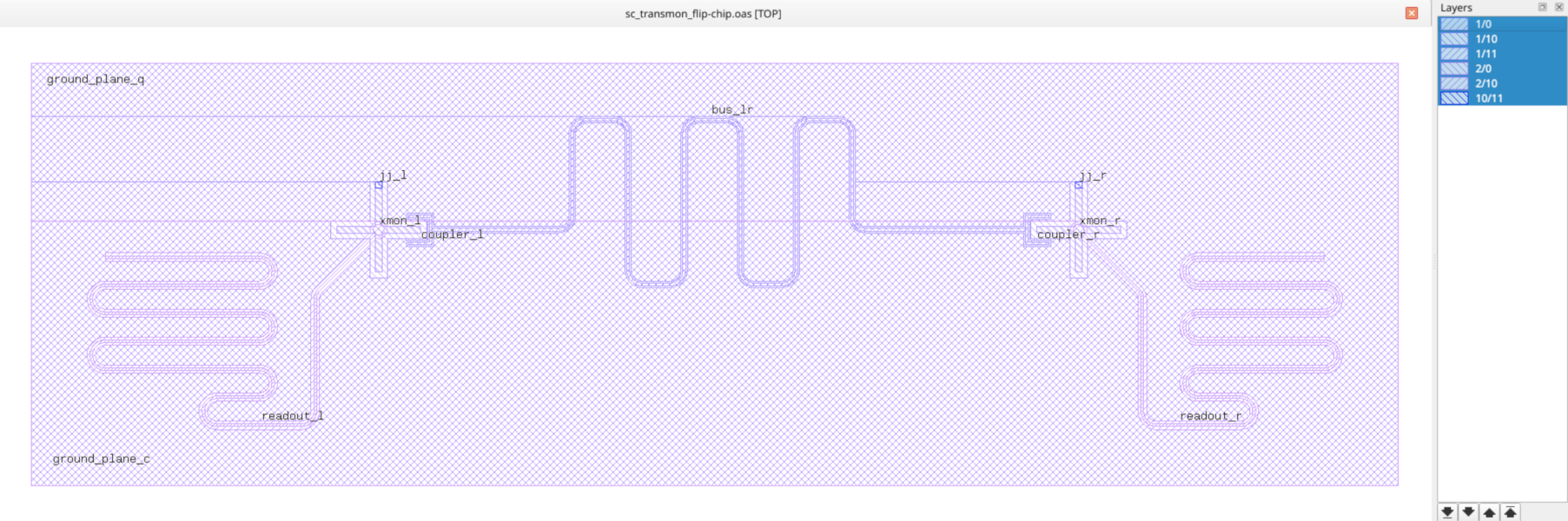
Fig. 2.2.3 Layout file opened in KLayout.
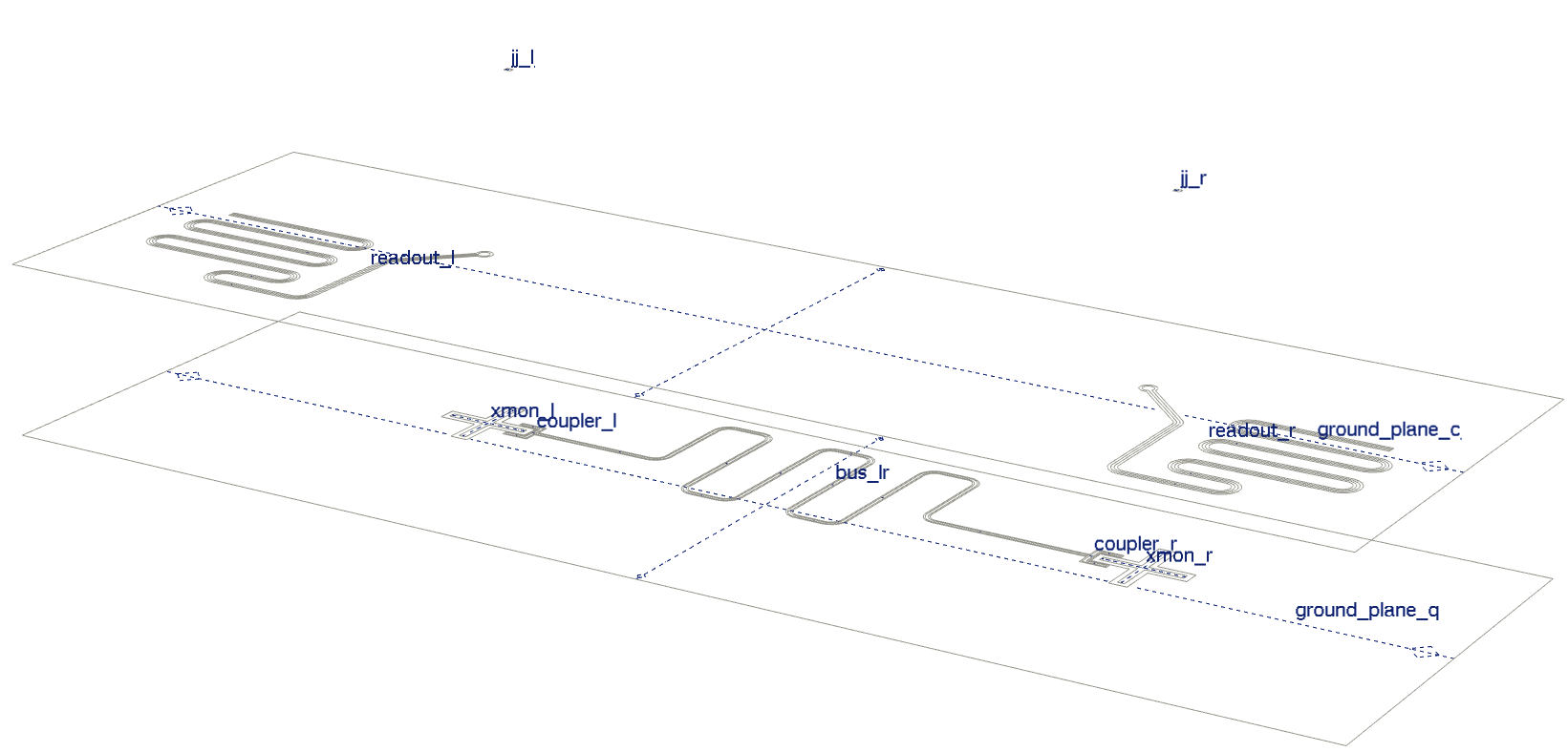
Fig. 2.2.4 Exploded view of the different layers (Q-chip, C-chip, junction ports) of the layout file.
Note that several of the steps found in this tutorial are similar to the ones found in the tutorial Coupled Xmons. Thus, we will shorten their discussion and focus on the specificities of the flip-chip architecture.
2.3. Setup
2.3.1. Header
We begin by importing the required modules and defining the working directories exactly as was done in the tutorial Coupled Xmons. We also define an auxiliary function to preview the geometry in Gmsh as we build the device.
from pathlib import Path
import numpy as np
from qtcad.builder import Builder, MeshAlgorithm3D

script_dir = Path(__file__).parent.resolve()
layout_dir = script_dir / "layouts"
mesh_dir = script_dir / "meshes"
out_dir = script_dir / "output"
out_dir.mkdir(exist_ok=True)

# Function to preview the geometry as we build the device.
# Change `flag_show` to `False` if you do not want the Gmsh window to be manually
# closed before proceeding
flag_show = True


def preview_geometry(
    builder,
    output_filepath,
    font_size=20,
    angles=(-45, 0, -15),
    show=flag_show,
):
    builder.view(
        surfaces=True,
        volume_labels=False,
        surface_labels=False,
        angles=angles,
        save=output_filepath,
        font_size=font_size,
        show=flag_show,
    )
2.3.2. Length scales and constants
We begin by setting the length scale for all geometric quantities to 1 μm. This scale factor will be used when loading the OAS file and in all subsequent Builder operations.
# Scale: 1 μm.
scale = 1e-6
Next, we define the separation of the chips (gap), the thickness of the dielectric substrates (assumed to be equal for both chips) and of the ‘air box’ that will surround the whole device.
# Gap between the Q and C chips.
gap = 10

# Thickness of the substrates.
thickness_substrate = 280

# Padding to add when enveloping the whole device in an air box.
airbox_padding_lateral = 200
airbox_padding_vertical = 300
Lastly, let us specify the target characteristic length of the mesh.
# Characteristic length of the mesh.
mesh_size = 300
2.4. Loading the layout
With an instantiated Builder object, let us load the
OASIS layout file specifying cell_name="TOP" to load the top-level cell of the
layout.
We also define a target characteristic length for the mesh.
# Instantiate Builder and load the layout file.
builder = Builder(name="transmon-chip", length_unit_exponent=int(np.log10(scale)))
builder.load_layout(layout_dir / "sc_transmon_flip-chip.oas", cell_name="TOP")

# Set mesh size.
builder.set_mesh_size(mesh_size)
Let us now check the loaded masks and their associated polygons.
# Show the list of layers and polygons.
builder.print_mask_tree()
Layout
├── Mask 10 "layer_10"
│   ├── 0  Polygon  "jj_l" (4)
│   └── 1  Polygon  "jj_r" (4)
├── Mask 1 "layer_1"
│   ├── 0  Polygon  "bus_lr" (968)
│   ├── 1  Polygon  "ground_plane_q" (1015)
│   ├── 2  Polygon  "xmon_l" (12)
│   ├── 3  Polygon  "coupler_r" (10)
│   ├── 4  Polygon  "coupler_l" (10)
│   └── 5  Polygon  "xmon_r" (12)
└── Mask 2 "layer_2"
    ├── 0  Polygon  "readout_r" (737)
    ├── 1  Polygon  "readout_l" (737)
    └── 2  Polygon  "ground_plane_c" (1467)
We see that the layout comprises three masks: the corresponding superconducting (SC) sheets for the Q- and C-chips as well as a layer with rectangles representing the Josephson junctions. Each of them hosts several named polygon objects associated with different components.
2.5. Building the chips
To construct the SC chip, we will merge and extrude the different elements to form the desired 3D geometry using the related Builder operations. Whilst several approaches are possible with Builder, here, we will first create the two SC sheets using the associated layers and add the rectangular ports representing the junctions to the Q-chip sheet. Next, we create the chip holders (substrates) for each chip and finish by adding an ‘air box’.
Since we will start with the creation of the chips, to guarantee that new entities will
inherit existing physical groups at intersections, such that previously named entities
will remain identifiable, we use Builder’s
fill_mode.
# Fill mode: new entities will inherit existing physical groups
# at intersections.
builder.fill_mode()
Also, as we add elements from the masks to the geometry, Builder will create addressable physical groups named following certain naming modes.
Furthermore, since each chip mask comprises several SC components individually labelled,
let us use group_from_shape.
This way, new entities will be assigned to a physical group that is named according to
the name of the shape from which that the entity is created.
# Make sure new entities created will be assigned to a physical group
# that is named according the source shape.
builder.group_from_shape()
Later, when adding the substrates and the air box, however, we will specify the
associated physical groups manually using
set_group_name.
2.5.1. SC sheets (Q-chip and C-chip) and Josephson junctions (lumped port, Q-chip)
We will represent both the thin SC structures and the rectangular ports representing Josephson junctions as 2D surfaces within the 3D geometry.
To do that, we will activate (‘use’) the relevant mask, defining an appropriate
z-coordinate for each, and add the elements using
add_surface.
Note
If we, however, were to consider the SC sheets as having a finite thickness, we would
replace add_surface by
extrude, passing the desired thickness.
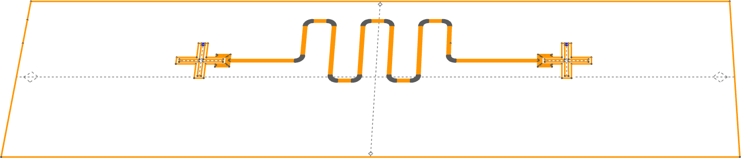
For the Q-chip, we will add, at \(z=-\mathtt{gap}/2\), the SC sheet (layer_1)
and the rectangular ports (layer_10).
# Move the z-coordinate to the position desired for the Q-chip’s SC surface.
builder.set_z(-gap / 2)

# Add all the elements of layer 1 (Q-chip, SC sheet).
builder.use_mask("layer_1")
builder.add_surface()

# Add the rectangular ports representing the junctions.
builder.use_mask("layer_10")
builder.add_surface()

preview_geometry(
    builder, out_dir / "builder_sc_transmon_flip-chip_step-1.png", angles=(-45, 0, 0)
)
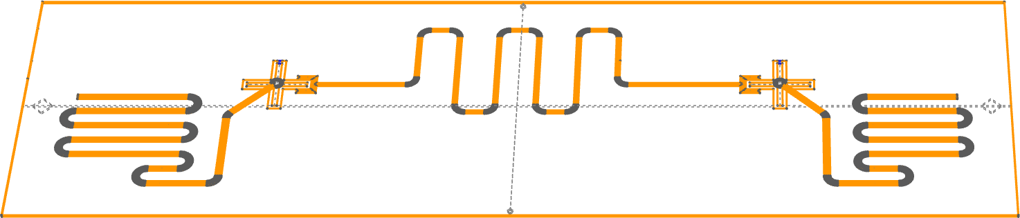
For the C-chip (layer_2), we will add its elements at \(z=+\mathtt{gap}/2\).
# Move the z-coordinate to the position desired for the C-chip’s SC surface.
builder.set_z(+gap / 2)

# Add all the elements of layer 2 (C-chip, SC sheet).
builder.use_mask("layer_2")
builder.add_surface()

preview_geometry(
    builder, out_dir / "builder_sc_transmon_flip-chip_step-2.png", angles=(-45, 0, 0)
)
2.5.2. Chip holders (Q-chip and C-chip)
Let us now add the substrate for both chips.
To do that, we will use the limits of the SC sheets to define the appropriate substrate
volumes via extrude_mask_bbox as done
in the tutorial Coupled Xmons.
Note that, contrary to the previous steps, where the physical groups created were
named automatically (group_from_shape),
here we will specify the associated physical groups manually to our liking using
set_group_name.
Let us then start by using the bounding box of the Q-chip layer ("layer_1") to create
its substrate by extruding it by -substrate_thick from \(z=-\mathtt{gap}/2\).
# Move the z-coordinate to the position desired for the Q-chip’s SC surface.
builder.set_z(-gap / 2)

# Extrudes the bounding box of layer 1 (Q-chip, SC sheet) to create the substrate.
builder.set_group_name("substrate_q")
builder.extrude_mask_bbox(height=-thickness_substrate, mask="layer_1")

preview_geometry(
    builder, out_dir / "builder_sc_transmon_flip-chip_step-3.png", angles=(-45, 0, -15)
)
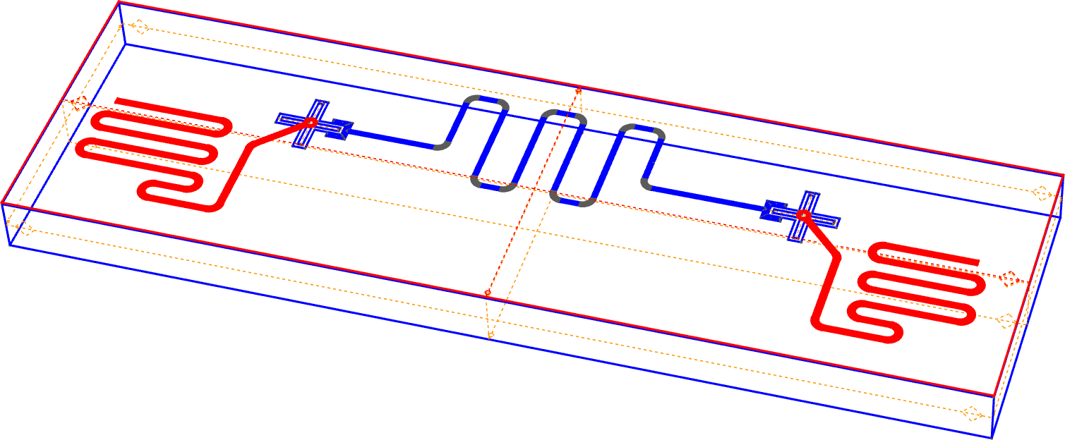
Next, let us do that same for the C-chip layer ("layer_2"), extruding its bounding box
by +substrate_thick from \(z=+\mathtt{gap}/2\).
# Move the z-coordinate to the position desired for the C-chip’s SC surface.
builder.set_z(+gap / 2)

# Extrude the bounding box of layer 2 (C-chip, SC sheet) to create the substrate.
builder.set_group_name("substrate_c")
builder.extrude_mask_bbox(height=+thickness_substrate, mask="layer_2")

preview_geometry(
    builder, out_dir / "builder_sc_transmon_flip-chip_step-4.png", angles=(-45, 0, -15)
)
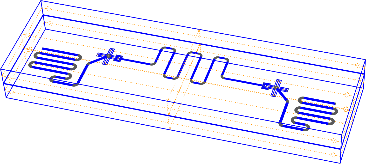
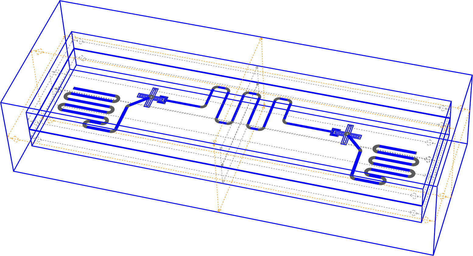
2.5.3. Air box
We can then envelop the whole device in an ‘air box’ using the wrap_in_bbox method
and the paddings previously defined.
The air box guarantees the presence of a meshed volume between the chips needed for
electromagnetic simulations.
# Envelop the whole device in an air box.
builder.set_group_name("air")
builder.wrap_in_bbox(
    padding=(airbox_padding_lateral, airbox_padding_lateral, airbox_padding_vertical)
)

preview_geometry(
    builder, out_dir / "builder_sc_transmon_flip-chip_step-5.png", angles=(-45, 0, -15)
)
2.6. Generating the mesh
Finally, we generate and export the 3D mesh using the HXT algorithm.
# Generate the mesh and save it.
builder.mesh(3, algorithm3d=MeshAlgorithm3D.HXT, show_gmsh_output=True)
builder.write(mesh_dir / "builder_sc_transmon_single.msh")
We also export a XAO geometry file, which is needed if we want to perform EM simulations using adaptive-mesh refinement.
# Export the geometry as an XAO file.
builder.write(mesh_dir / "builder_sc_transmon_flip-chip.xao")
Lastly, let us visualize the generated mesh.
# Visualize the mesh.
builder.view(
    surfaces=False,
    volume_labels=True,
    angles=(-45, 0, -15),
    save=str(out_dir / "builder_sc_transmon_flip-chip_mesh.png"),
)
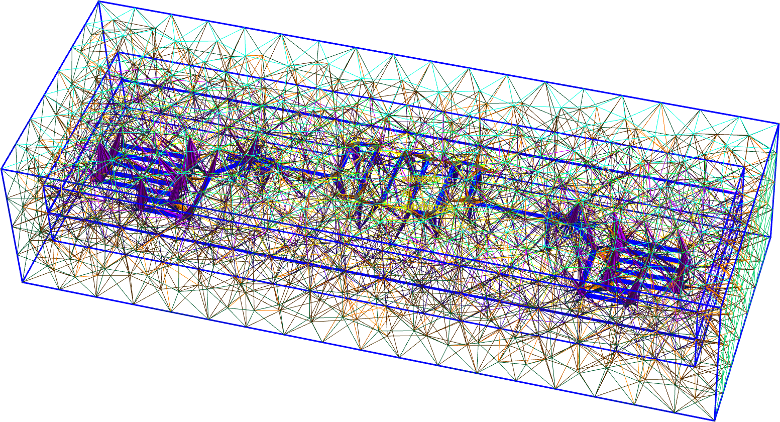
Fig. 2.6.7 Final 3D mesh of the device.
The generated geometry and mesh files can then be used to run electromagnetic simulations using QTCAD. This is not covered in this tutorial, but the interested reader is referred to Device package (superconducting circuits). There, we present examples of the different types of simulation and analyses than can be performed using QTCAD.
2.7. Full code
__copyright__ = "Copyright 2022-2026, Nanoacademic Technologies Inc."

from pathlib import Path
import numpy as np
from qtcad.builder import Builder, MeshAlgorithm3D

script_dir = Path(__file__).parent.resolve()
layout_dir = script_dir / "layouts"
mesh_dir = script_dir / "meshes"
out_dir = script_dir / "output"
out_dir.mkdir(exist_ok=True)
# Function to preview the geometry as we build the device.
# Change `flag_show` to `False` if you do not want the Gmsh window to be manually
# closed before proceeding
flag_show = True


def preview_geometry(
    builder,
    output_filepath,
    font_size=20,
    angles=(-45, 0, -15),
    show=flag_show,
):
    builder.view(
        surfaces=True,
        volume_labels=False,
        surface_labels=False,
        angles=angles,
        save=output_filepath,
        font_size=font_size,
        show=flag_show,
    )


# Scale: 1 μm.
scale = 1e-6

# Gap between the Q and C chips.
gap = 10

# Thickness of the substrates.
thickness_substrate = 280

# Padding to add when enveloping the whole device in an air box.
airbox_padding_lateral = 200
airbox_padding_vertical = 300

# Characteristic length of the mesh.
mesh_size = 300

# Instantiate Builder and load the layout file.
builder = Builder(name="transmon-chip", length_unit_exponent=int(np.log10(scale)))
builder.load_layout(layout_dir / "sc_transmon_flip-chip.oas", cell_name="TOP")

# Set mesh size.
builder.set_mesh_size(mesh_size)

# Show the list of layers and polygons.
builder.print_mask_tree()

# Fill mode: new entities will inherit existing physical groups
# at intersections.
builder.fill_mode()

# Make sure new entities created will be assigned to a physical group
# that is named according the source shape.
builder.group_from_shape()

# Move the z-coordinate to the position desired for the Q-chip’s SC surface.
builder.set_z(-gap / 2)

# Add all the elements of layer 1 (Q-chip, SC sheet).
builder.use_mask("layer_1")
builder.add_surface()

# Add the rectangular ports representing the junctions.
builder.use_mask("layer_10")
builder.add_surface()

preview_geometry(
    builder, out_dir / "builder_sc_transmon_flip-chip_step-1.png", angles=(-45, 0, 0)
)


# Move the z-coordinate to the position desired for the C-chip’s SC surface.
builder.set_z(+gap / 2)

# Add all the elements of layer 2 (C-chip, SC sheet).
builder.use_mask("layer_2")
builder.add_surface()

preview_geometry(
    builder, out_dir / "builder_sc_transmon_flip-chip_step-2.png", angles=(-45, 0, 0)
)

# Move the z-coordinate to the position desired for the Q-chip’s SC surface.
builder.set_z(-gap / 2)

# Extrudes the bounding box of layer 1 (Q-chip, SC sheet) to create the substrate.
builder.set_group_name("substrate_q")
builder.extrude_mask_bbox(height=-thickness_substrate, mask="layer_1")

preview_geometry(
    builder, out_dir / "builder_sc_transmon_flip-chip_step-3.png", angles=(-45, 0, -15)
)

# Move the z-coordinate to the position desired for the C-chip’s SC surface.
builder.set_z(+gap / 2)

# Extrude the bounding box of layer 2 (C-chip, SC sheet) to create the substrate.
builder.set_group_name("substrate_c")
builder.extrude_mask_bbox(height=+thickness_substrate, mask="layer_2")

preview_geometry(
    builder, out_dir / "builder_sc_transmon_flip-chip_step-4.png", angles=(-45, 0, -15)
)

# Envelop the whole device in an air box.
builder.set_group_name("air")
builder.wrap_in_bbox(
    padding=(airbox_padding_lateral, airbox_padding_lateral, airbox_padding_vertical)
)

preview_geometry(
    builder, out_dir / "builder_sc_transmon_flip-chip_step-5.png", angles=(-45, 0, -15)
)

# Generate the mesh and save it.
builder.mesh(3, algorithm3d=MeshAlgorithm3D.HXT, show_gmsh_output=True)
builder.write(mesh_dir / "builder_sc_transmon_single.msh")

# Export the geometry as an XAO file.
builder.write(mesh_dir / "builder_sc_transmon_flip-chip.xao")

# Visualize the mesh.
builder.view(
    surfaces=False,
    volume_labels=True,
    angles=(-45, 0, -15),
    save=str(out_dir / "builder_sc_transmon_flip-chip_mesh.png"),
)