1. From photomask to mesh generation
1.1. Requirements
1.1.1. Software components
QTCAD
devicegen
Gmsh
1.1.2. Layout file
qtcad/examples/practical_application/layouts/gated_qd.txt
1.1.3. Python script
qtcad/examples/practical_application/1-devicegen.py
1.1.4. References
1.2. Briefing
As described in Devicegen, devicegen is an open-source code
that was developed by Nanoacademic to generate a
device and its mesh from a photomask layout
(a GDS-TXT file produced by layout editors such as
KLayout).
The aim of this tutorial is to demonstrate how devicegen can be used to accelerate the generation of meshes appropriate for modelling semiconductor nanodevices. This circumvents the need to generate device meshes using Gmsh, as was done for the Tutorials and Tutorials. Here, the demonstration is made for the following gated quantum-dot system:
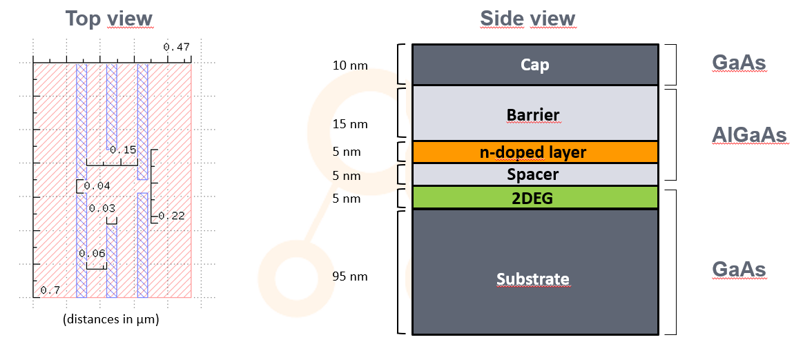
Fig. 1.2.1 Top and side views of the quantum dot under consideration
The left-hand side of the above figure shows the layout for this example
device, which can be found in examples/practical_application/layouts/gated_qd.txt.
This layout file is in .txt format and can be visualized and modified
using, e.g. KLayout. In the above picture,
the red rectangle represents the simulation domain, while the blue
rectangles represent metallic gates deposited on top of the chip that
are used to control the confinement potential used to achieve
confinement of single charge carriers in the \(x\)–\(y\) plane.
The right-hand side of the above figure illustrates the heterostructure
stack, i.e. the multiple layers of materials used to confine charge
carriers in the \(z\) direction. Each layer will be labeled differently to
represent the role it plays in the heterostructure, and will be assigned
a certain number of mesh layers depending on how accurate the simulation
should be in each region (assuming a static mesh). In this example,
the mismatch between conduction band edges of GaAs and AlGaAs is used to form
a Barrier isolating electrons in the substrate from the Cap region,
and an n-doped layer is used to bend the conduction band edge and form a
triangular confinement potential in the region indicated as 2DEG in
the above figure. Finally, a Spacer region is used to isolate the
quantum dot formed in the 2DEG from the dopants.
1.3. Setup
1.3.1. Header
To generate the mesh for the gated quantum dot using devicegen, we start by importing two relevant modules
from devicegen import DeviceGenerator
import pathlib
The first import is the DeviceGenerator, while the second is the
standard Python library pathlib which will be used to facilitate
referencing files.
1.3.2. Heterostructure stack specifications
Next we define some constants that will be useful in setting up the
device in the subsequent steps. In devicegen, all lengths are given
in micrometers, so that we convert from nanometers to micrometers by
multiplying by 1e-3.
# Constants
# # Mesh characteristic lengths
char_len = 15 * 1e-3
dot_char_len = char_len/2

## z dimensions
### Thickness of each material layer
cap_thick = 10 * 1e-3
barrier_thick = 15 * 1e-3
dopant_thick = 5 * 1e-3
spacer_thick = 5 * 1e-3
two_deg_thick = 5 * 1e-3
substrate_thick = 100 * 1e-3 - two_deg_thick

### Number of mesh points along growth axis
cap_layers = 5
barrier_layers = 5
dopant_layers = 10
spacer_layers = 10
two_deg_layers = 10
substrate_layers = 10
1.3.3. Load layout
The final step of the setup is to load the layout of the device in the
DeviceGenerator. The layout can be imported as either a .geo file or
a .gds file saved with the .txt extension. In this example we will load
the .txt file found in examples/practical_application/layouts/gated_qd.txt.
Saving a layout into a GDS-TXT file with .txt extension should be
straightforward with most layout editors. For example, in KLayout, this is
done using File → Save As by selecting GDS2 Text files in the drop-down menu
'Type' under the file name field.
# Initializing the DeviceGenerator
script_dir = pathlib.Path(__file__).parent.resolve()
file = str(script_dir / "layouts" / "gated_qd.txt")
outfile = str(script_dir / "layouts" / "gated_qd.geo")
dG = DeviceGenerator(file, outfile=outfile, h=char_len)
The constructor DeviceGenerator has one required argument and
multiple optional arguments. The only required argument is the path to
the file containing the layout. In our case, it is the .txt file stored
in file. If a .txt file is loaded, the DeviceGenerator
automatically creates a corresponding .geo file, named parsed.geo by
default, containing the same information. The path and the name of
the output .geo file can be specified in the optional input outfile.
The optional input h controls the characteristic length of the mesh
generated over the layout. The characteristic lengths at different
points can further be altered later on using, e.g. the new_box_field
method of the DeviceGenerator (see
the open-source devicegen repository).
The layout can be viewed within the Gmsh GUI by running
# visualization
dG.view()
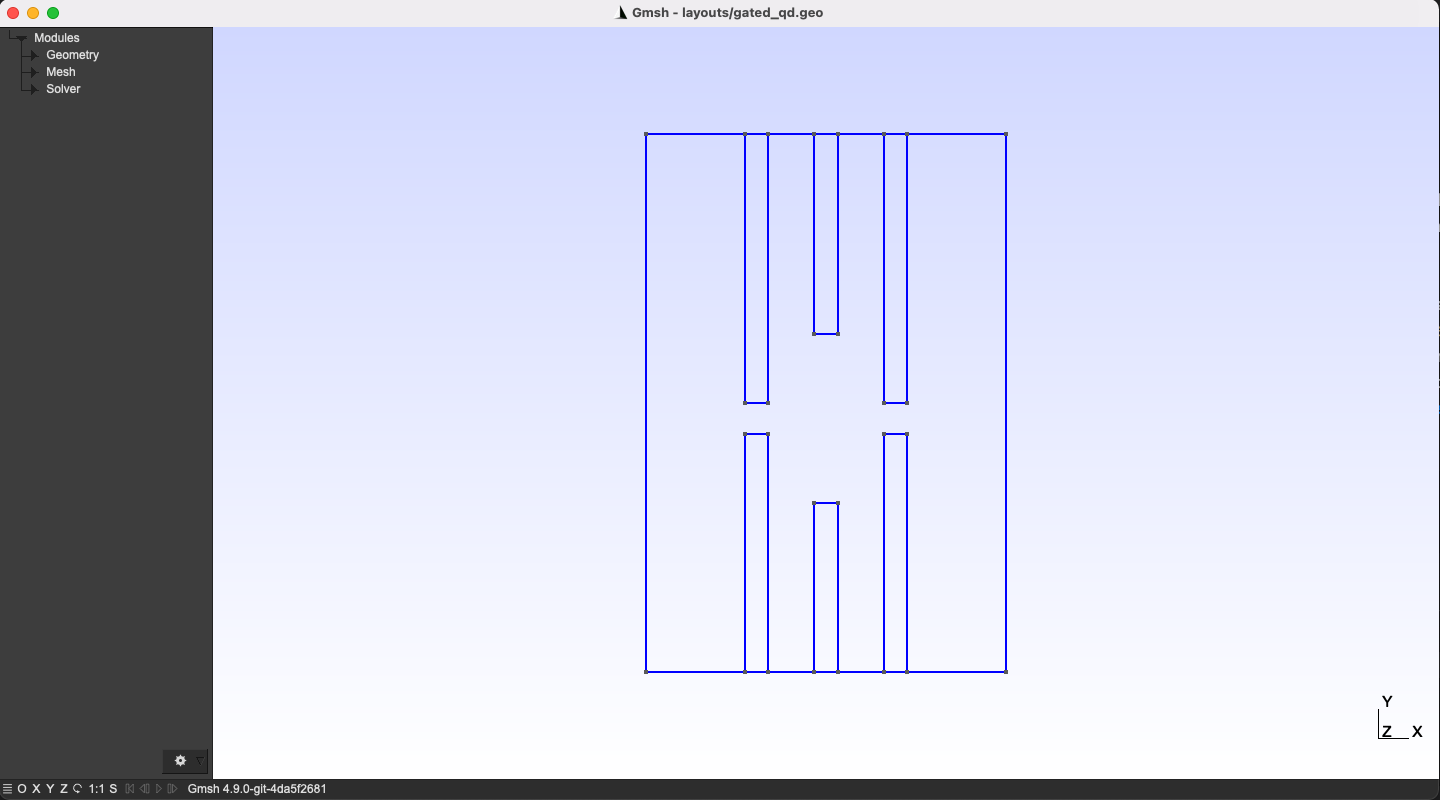
Fig. 1.3.3 Layout of the device which exhibits the structure of the gates
1.4. Creating a dot region
The DeviceGenerator allows users to create rectangles in the layout
where they expect a quantum dot to be formed. This is achieved using the
new_dot_rectangle method.
# Dot rectangle coordinates in microns
dot_xmin = 0.16900;  dot_ymin = 0.23100
dot_len_x = 0.131; dot_len_y = 0.197
dG.new_dot_rectangle(dot_xmin, dot_ymin, dot_len_x, dot_len_y,
    h=dot_char_len)
This method has four arguments and an optional argument. The arguments
are the minimal \(x\) and \(y\) values of the “dot rectangle” and its
lengths in the \(x\) and \(y\) directions. In this example, these are
given by the constants: dot_xmin, dot_ymin, dot_len_x, and
dot_len_y, respectively. Recall that the units of length used by the device
generator are microns. Finally, there is also the optional input h
which sets the characteristic length of the mesh within the dot
rectangle.
Again, we can visualize the model thus far with the view method.
# Display layout with dot region
dG.view()
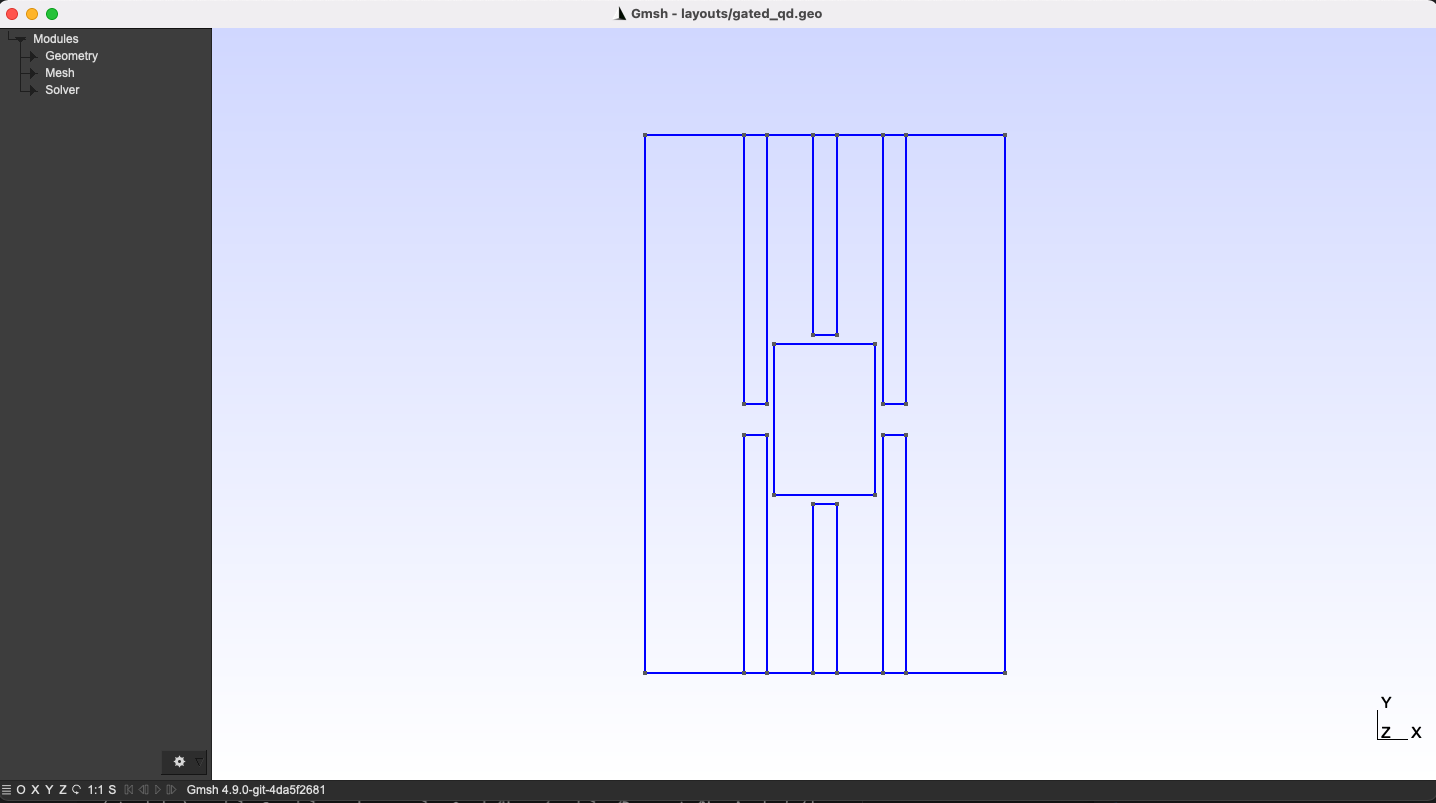
Fig. 1.4.5 Device layout including a dot region
The DeviceGenerator has added a rectangular surface to the layout.
Another byproduct of using the DeviceGenerator is that all the
surfaces have been attributed a name (a “physical surface” name, in the
language of Gmsh). To see the names of each surface we can select
Tools → Options:
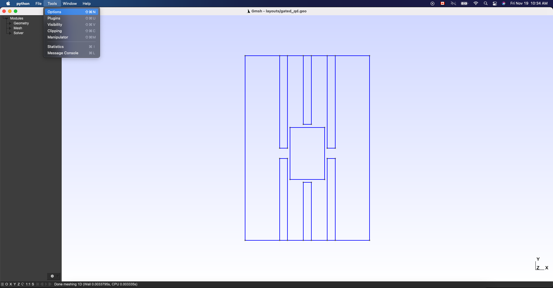
Fig. 1.4.6 Navigating to the Tools → Options menu
The following window should pop up:
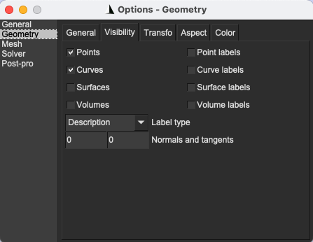
Fig. 1.4.7 The geometry menu
from which the Geometry tab should be selected. Then, we check the box Surface labels and in the dropdown menu Label type select Physical name(s):
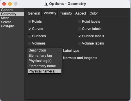
Fig. 1.4.8 Viewing physical surfaces
Once these selections have been made, we should see the name of each surface.
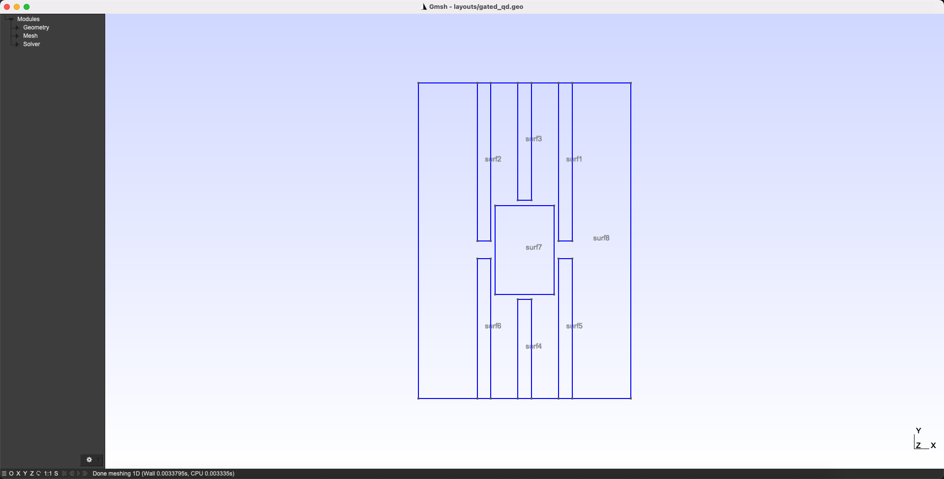
Fig. 1.4.9 Device layout including the default physical surface labels
We can also visualize the 2D mesh on the layout by pressing the 2 key on the keyboard or by clicking Mesh > 2D in the Gmsh GUI.
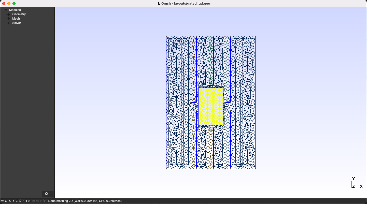
Fig. 1.4.10 Device layout mesh
The mesh within the dot region should be twice as fine as outside the dot region.
Note
There are three main reasons why a dot region should always be defined:
A finer mesh may be required inside the dot region for improved Schrödinger solver accuracy.
The nodes outside the dot region are typically irrelevant to quantum dot physics; we only need to solve the Schrödinger equation inside the local potential well(s) forming the quantum dot system. Solving anywhere else would be a waste of computational resources.
The Schrödinger solver will find the first energy levels near the global confinement potential energy minimum. When the solver is defined for the entire device geometry, if the potential energy within the quantum-dot region is only at a local minimum, then the Schrödinger equation eigensolutions will display a probability density that is concentrated outside the dot region. In situations where the global minimum lies in classical regions (e.g., in classical electron or hole reservoirs), defining a dot region thus becomes a necessity—otherwise, physically irrelevant solutions will be output by the Schrödinger solver.
1.5. Relabelling surfaces
The relabel_surface method allows us to relabel the surfaces which
have been automatically assigned generic names. Here we distinguish three
top gates from three bottom gates.
# Relabelling surfaces
print('Relabelling surfaces...')
dG.relabel_surface('surf2', 'top_gate_1')
dG.relabel_surface('surf3', 'top_gate_2')
dG.relabel_surface('surf1', 'top_gate_3')
dG.relabel_surface('surf6', 'bottom_gate_1')
dG.relabel_surface('surf4', 'bottom_gate_2')
dG.relabel_surface('surf5', 'bottom_gate_3')

# Display layout with relabelled surfaces
dG.view()
The first input of the relabel_surface method is the old name of the
surface and the second input is its new name. This method has additional
optional inputs that allows users to set some metadata for each surface
which can define the boundary conditions at the surface (see
the open-source devicegen repository).
Using the same procedure described above, the surface labels can be shown to be:
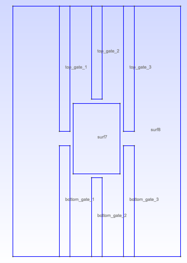
Fig. 1.5.5 Relabelled surfaces
1.6. Setting up the heterostructure stack
Now that the 2D geometry has been addressed, we focus on creating the
heterostructure stack. This is taken care of using the new_layer
method.
# Heterostructure stack
print('Setting up heterostructure stack...')
dG.new_layer(cap_thick, cap_layers, label='cap')
dG.new_layer(barrier_thick, barrier_layers, label='barrier')
dG.new_layer(dopant_thick, dopant_layers, label='dopant_layer')
dG.new_layer(spacer_thick, spacer_layers, label='spacer_layer',
    dot_region=True, dot_label="spacer_dot")
dG.new_layer(two_deg_thick, two_deg_layers, label='two_deg',
    dot_region=True, dot_label="two_deg_dot")
dG.new_layer(substrate_thick, substrate_layers, label='substrate',
    dot_region=True, dot_label="substrate_dot")

# Display heterostructure stack
dG.view()
This method has two inputs that indicate how thick each layer is and how
fine the mesh is within this layer along the growth direction. This
second input is given as an integer which tells the Gmsh extrude
function how many times to copy the layout along the growth direction to
create the mesh (see
here
or
here
for more details). The optional label input allows us to label the
volume created by the layer. Though this is optional, it is strongly
recommended to define such a label because each physical region must be
assigned a material in QTCAD (it may be more difficult to retrieve specific
regions if default labels are used). For some layers we have also specified
dot_region = True and given a dot_label. These optional inputs
allow us to separate the dot region in the layers from the rest of the
layer and give the dot region a separate label. This could be useful,
e.g. if we want to model the dot region differently from the rest of the
device (e.g. treating the dot region quantum mechanically but the rest
of the device classically). The new_layer method has multiple
additional optional inputs that may be used to add metadata (such as the
material and the doping) to each volume (see
the open-source devicegen repository
for more details). This metadata is saved in the DeviceGenerator object,
but not in the mesh file. Consequently, it will not be seen by QTCAD.
Following the same steps as when we wanted to display the surface
labels, we can also display volume labels. Using the Gmsh GUI to
move around and zoom, it should be clear that the dot volumes in the
spacer, two_deg, and substrate layers have a separate name.
Tip: It may be easier to read the physical group label using the dark interface of the Gmsh GUI. To activate or deactivate the dark interface: Gmsh GUI → Tools → Options → General → General → Use dark interface.
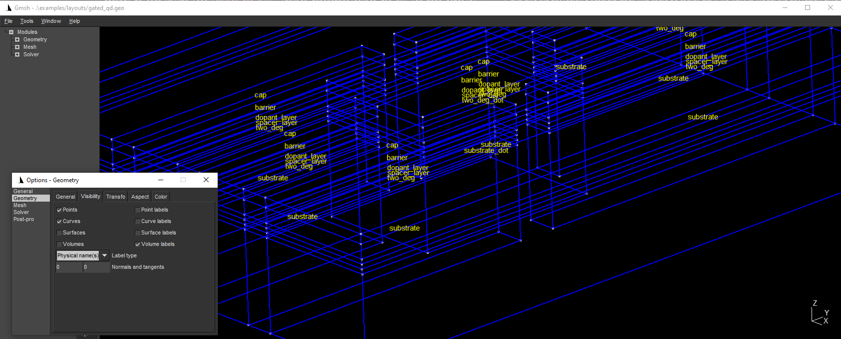
Fig. 1.6.1 Device and its labelled volumes
1.7. Defining a boundary condition at the bottom of the device
We can also set up a label for the entire surface at the bottom of the device
using the label_bottom method
print('Setting up back gate...')
dG.label_bottom('ohmic_bnd')

# Display final layout
dG.view()
This method will label the bottom surface with the string given to it as input.
1.8. Saving the mesh
Finally, we can save the mesh generated from the instructions above to
the disk using the save_mesh method
# Save mesh
mesh_name = str(script_dir/"meshes"/"gated_dot.msh")
dG.save_mesh(mesh_name = mesh_name)
Here the mesh_name input gives the path and name of the output mesh.
By default, the output mesh will be saved in a file named mesh.msh.
However, here we have specified that the output mesh should be saved to
the meshes directory under the name gated_dot.msh. The file
extension (in this case .msh) will determine under which format the
mesh is saved.
1.9. Full code
__copyright__ = "Copyright 2022-2025, Nanoacademic Technologies Inc."

from devicegen import DeviceGenerator
import pathlib

# Constants
# # Mesh characteristic lengths
char_len = 15 * 1e-3
dot_char_len = char_len/2

## z dimensions
### Thickness of each material layer
cap_thick = 10 * 1e-3
barrier_thick = 15 * 1e-3
dopant_thick = 5 * 1e-3
spacer_thick = 5 * 1e-3
two_deg_thick = 5 * 1e-3
substrate_thick = 100 * 1e-3 - two_deg_thick

### Number of mesh points along growth axis
cap_layers = 5
barrier_layers = 5
dopant_layers = 10
spacer_layers = 10
two_deg_layers = 10
substrate_layers = 10

# Initializing the DeviceGenerator
script_dir = pathlib.Path(__file__).parent.resolve()
file = str(script_dir / "layouts" / "gated_qd.txt")
outfile = str(script_dir / "layouts" / "gated_qd.geo")
dG = DeviceGenerator(file, outfile=outfile, h=char_len)

# visualization
dG.view()

# Dot rectangle coordinates in microns
dot_xmin = 0.16900;  dot_ymin = 0.23100
dot_len_x = 0.131; dot_len_y = 0.197
dG.new_dot_rectangle(dot_xmin, dot_ymin, dot_len_x, dot_len_y,
    h=dot_char_len)

# Display layout with dot region
dG.view()

# Relabelling surfaces
print('Relabelling surfaces...')
dG.relabel_surface('surf2', 'top_gate_1')
dG.relabel_surface('surf3', 'top_gate_2')
dG.relabel_surface('surf1', 'top_gate_3')
dG.relabel_surface('surf6', 'bottom_gate_1')
dG.relabel_surface('surf4', 'bottom_gate_2')
dG.relabel_surface('surf5', 'bottom_gate_3')

# Display layout with relabelled surfaces
dG.view()

# Heterostructure stack
print('Setting up heterostructure stack...')
dG.new_layer(cap_thick, cap_layers, label='cap')
dG.new_layer(barrier_thick, barrier_layers, label='barrier')
dG.new_layer(dopant_thick, dopant_layers, label='dopant_layer')
dG.new_layer(spacer_thick, spacer_layers, label='spacer_layer',
    dot_region=True, dot_label="spacer_dot")
dG.new_layer(two_deg_thick, two_deg_layers, label='two_deg',
    dot_region=True, dot_label="two_deg_dot")
dG.new_layer(substrate_thick, substrate_layers, label='substrate',
    dot_region=True, dot_label="substrate_dot")

# Display heterostructure stack
dG.view()

print('Setting up back gate...')
dG.label_bottom('ohmic_bnd')

# Display final layout
dG.view()

# Save mesh
mesh_name = str(script_dir/"meshes"/"gated_dot.msh")
dG.save_mesh(mesh_name = mesh_name)