2. Simulating bound states in a quantum dot using the Poisson and Schrödinger solvers
2.1. Requirements
2.1.1. Software components
QTCAD
2.1.2. Mesh file
qtcad/examples/practical_application/meshes/gated_dot.msh
2.1.3. Python script
qtcad/examples/practical_application/2-poisson_schrodinger.py
2.1.4. References
2.2. Briefing
In the previous tutorial, we have used devicegen to generate
a .msh file describing the geometry and mesh of a gated
heterostructure stack. This is a structure used in practice to
confine charge carriers to a finite volume of space, namely a quantum dot.
In this tutorial, we will use QTCAD to calculate this quantum dot’s bound
states eigenenergies and eigenstates. We will do so by
obtaining the dot’s confinement potential by solving the (classical) nonlinear Poisson equation throughout the entire device;
solving the Schrödinger equation within the dot.
2.3. Setting up the device
2.3.1. Header
We start by importing the relevant modules.
from qtcad.device import constants as ct
from qtcad.device.mesh3d import Mesh, SubMesh
from qtcad.device import io
from qtcad.device import materials as mt
from qtcad.device import Device, SubDevice
from qtcad.device.poisson import Solver as PoissonSolver
from qtcad.device.poisson import SolverParams as PoissonSolverParams
from qtcad.device.schrodinger import Solver as SchrodingerSolver
from qtcad.device import analysis as an

import pathlib
These modules were seen in some tutorials, notably Poisson and Schrödinger simulation of a nanowire quantum dot and Schrödinger equation for a quantum dot. Importantly, both the Mesh and SubMesh classes are imported; the former will model and store information about the mesh of the entire gated heterostructure stack, while the latter will only do so for a subset of the full mesh (here the quantum dot).
2.3.2. Loading the mesh, defining material composition, and applying external voltages
First, the heterostructure device is created from the mesh.
# Input file
script_dir = pathlib.Path(__file__).parent.resolve()
path_mesh = str(script_dir/'meshes'/'gated_dot.msh')

# Load the mesh
scaling = 1e-6
mesh = Mesh(scaling,path_mesh)
mesh.show()

# Create device
d = Device(mesh, conf_carriers="e")
d.set_temperature(0.1)
Note that the temperature was set to be equal to \(0.1\textrm{ K}\)
using the set_temperature method, instead of the default temperature
(\(300\;\textrm K\)).
In addition, remark that scaling is set to \(10^{-6}\), because length
units in QTCAD are SI base units (meters), while they are micrometers in
devicegen (in accordance with most layout editors).
Finally, the conf_carriers attribute of the Device object d was set
to "e", meaning that the Schrödinger equation solver, which will be used
later in this tutorial, will compute the electron envelope function (but not
the hole envelope functions).
Next, the material composition of the heterostructure is specified.
# Ionized dopant density
doping = 3e18*1e6   # In SI units

# Set up materials in heterostructure stack
d.new_region("cap", mt.GaAs)
d.new_region("barrier", mt.AlGaAs)
d.new_region("dopant_layer", mt.AlGaAs,ndoping=doping)
d.new_region("spacer_layer", mt.AlGaAs)
d.new_region("spacer_dot", mt.AlGaAs)
d.new_region("two_deg", mt.GaAs)
d.new_region("two_deg_dot", mt.GaAs)
d.new_region("substrate", mt.GaAs)
d.new_region("substrate_dot", mt.GaAs)
For example, the physical volume labeled by dopant_layer in the .msh file
is defined to be composed of n-doped AlGaAs with a dopant concentration
of \(3\times 10^{18}\textrm{ cm}^{-3}\). By default, the ionization model
is complete ionization—all dopants will thus be assumed to be ionized.
By default, in QTCAD, band alignments across heterojunctions are computed using Anderson’s rule. While this rule is simple and widely applicable, it often fails to accurately predict band alignments. Indeed, Anderson’s rule ignores interface physics which may play a significant role in band alignment, such as interface dipoles and Fermi level pinning. The QTCAD team has modeled such physics in density-functional-theory simulations to more accurately predict band alignments across certain common heterojunctions, notably GaAs/AlGaAs heterojunctions (see the Band alignment in heterostructures theory section and the Band alignment in heterostructures tutorial). To harness these results that go beyond Anderson’s rule, you may simply execute the following.
# Align the bands across hetero-interfaces using GaAs as the reference material
d.align_bands(mt.GaAs)
Here, GaAs is taken to be the reference material—i.e., ab initio band alignments with respect to GaAs are used. Such ab initio band alignments are currently only available for GaAs/AlGaAs heterostructures.
Next, we forbid any charge, either classical or quantum, from forming in the
"cap" and "barrier" regions. This is done using the new_insulator
method of the device d.
# Remove unphysical charge from cap and barrier
d.new_insulator("cap")
d.new_insulator("barrier")
If these two lines were omitted from the code, a secondary 2DEG
would form across the cap–barrier interface, which would greatly affect the
potential profile and charge density within the primary 2DEG, across the
spacer–substrate interface. In typical experimental devices, only the primary
2DEG would be connected to thermal reservoirs (electrodes) able to supply
electrons and/or holes to the device. Thus, to reach the secondary 2DEG,
electrons would need to tunnel across around \(30~\textrm{nm}\) of AlGaAs,
namely across the spacer, doped, and barrier layers of the heterostructure. The
corresponding tunneling probability would be extremely low, leading to an
extremely low electron density across the secondary 2DEG, thereby justifying
our use of the new_insulator method.
Finally, we set the values of external voltages.
# Applied potentials
Vtop_1 = -0.5
Vtop_2 = -0.5
Vtop_3 = -0.5
Vbottom_1 = -0.5
Vbottom_2 = -0.5
Vbottom_3 = -0.5

# Work function of the metallic gates at midgap of GaAs
barrier = 0.834*ct.e    # n-type Schottky barrier height

# Set up boundary conditions
d.new_schottky_bnd("top_gate_1", Vtop_1, barrier)
d.new_schottky_bnd("top_gate_2", Vtop_2, barrier)
d.new_schottky_bnd("top_gate_3", Vtop_3, barrier)
d.new_schottky_bnd("bottom_gate_1", Vbottom_1, barrier)
d.new_schottky_bnd("bottom_gate_2", Vbottom_2, barrier)
d.new_schottky_bnd("bottom_gate_3", Vbottom_3, barrier)
d.new_ohmic_bnd("ohmic_bnd")
For example, a Schottky boundary condition is set on the physical
surface labelled as top_gate_1. To do so, the new_schottky_bnd
method is called, which takes as arguments the surface label, the
applied voltage (V_top_1), and the Schottky barrier height (barrier)
across the semiconductor–gate (GaAs–metal) junction. Mathematically, this
corresponds to a Dirichlet boundary condition with a boundary value
determined by V_top_1 and barrier, but for which the actual potential
value also accounts for Schottky physics. Note that here, we use the n-type
Schottky barrier height for aluminium on GaAs. Similarly, an Ohmic
boundary condition is set on the whole bottom surface of the device
using the new_ohmic_bnd method. It also corresponds to a Dirichlet
boundary condition; the boundary value is determined by the material
composition and doping of the nodes on the boundary. See the
Boundary Conditions theory section for more information about available
conditions and their corresponding equations.
2.4. Solving the nonlinear Poisson equation in the heterostructure
Now that the material composition of the device and the external voltages have been specified, we solve the nonlinear Poisson equation. We are especially interested in the potential in and around the quantum dot region, since this confining potential will be used to compute the bound states of the quantum dot.
First, we instantiate the solver parameters and the corresponding non-linear Poisson solver, as was done in Poisson and Schrödinger simulation of a nanowire quantum dot.
# Create the non-linear Poisson solver and set its parameters
solver_params = PoissonSolverParams({"tol": 1e-3, "maxiter": 100})
poisson_solver = PoissonSolver(d, solver_params=solver_params)
The default solver parameter values for the Poisson solver are used, with
the exceptions that the convergence threshold is set to tol = 1e-3 and
that the maximum number of iterations is set to maxiter = 100.
Next, we define the submesh corresponding to the quantum dot region
# Create a submesh including only the dot region
submesh = SubMesh(mesh, ["spacer_dot","two_deg_dot","substrate_dot"])
submesh.show()
In this case, the quantum dot is the union of the regions labeled by
spacer_dot, two_deg_dot, and substrate_dot. It is important to
include not only the physical region within the 2DEG part of the structure,
but also in the regions above and below. This is because a potential well
must be clearly defined along the \(z`\) direction for quantum confinement
to be correctly modelled. In particular, if the spacer_dot region is not
included, the potential barrier at the GaAs/AlGaAs interface will be missing
in the dot region, and the output solutions of the Schrödinger solver will be
wrong.
Next, the
set_dot_region
method is called on the device object d. This
sets the classical charge distribution to be zero in the quantum dot
region; indeed, charge in this region will later be treated quantum
mechanically by solving the Schrödinger equation.
# Set up the dot region in which no classical charge is allowed
d.set_dot_region(submesh)
Next, the nonlinear Poisson equation is solved in d, i.e. the
self-consistent iteration described in Non-linear Poisson solver is executed
until convergence.
# Solve
poisson_solver.solve()
Finally, the results are saved in .vtu files for visualization.
# Save the conduction band edge in .vtu format
outfile_cond_band_edge = str(script_dir / "output" / "cond_band_edge.vtu")
out_dict = {"EC (eV)": d.cond_band_edge()/ct.e}
io.save(outfile_cond_band_edge, out_dict, mesh)

# Save the electron density in .vtu format
outfile_electron_dens = str(script_dir / "output" / "electron_dens.vtu")
out_dict = {"n (1/m^3)": d.n}
io.save(outfile_electron_dens, out_dict, mesh)
For example, the figure below shows a side view of the electron density.
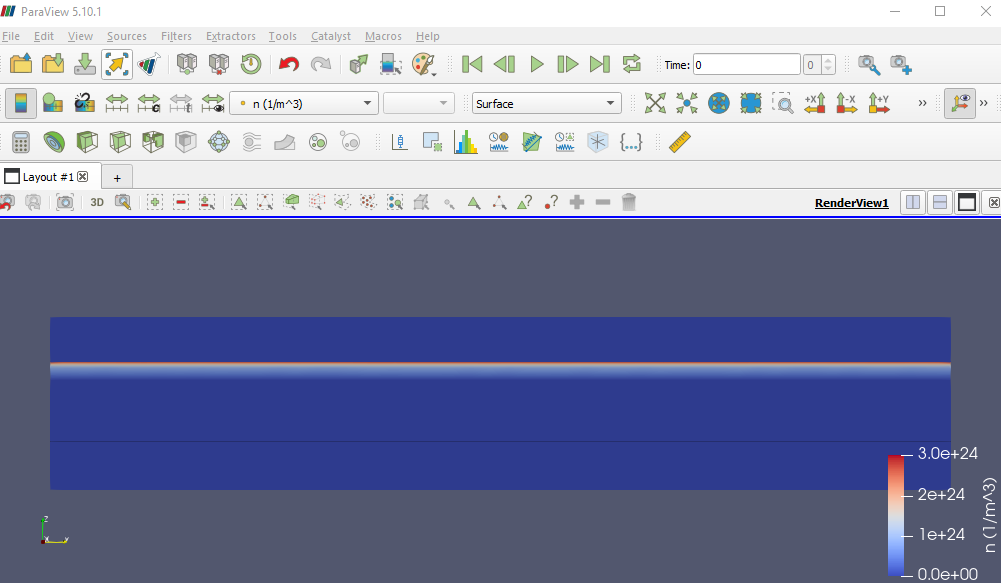
Fig. 2.4.11 Electron density
2.5. Solving Schrödinger’s equation in the quantum dot
It remains to compute the eigenenergies and eigenstates of the bound states
in the quantum dot. To do so, first, the potential energy profile is computed
and stored in the device d.
# Get the potential energy from the band edge for usage in the Schrodinger
# solver
d.set_V_from_phi()
Next, a subdevice for the quantum dot is created; a Schrödinger equation solver is defined for this subdevice.
# Create a subdevice for the dot region
subdevice = SubDevice(d,submesh)

# Create a Schrodinger solver
schrod_solver = SchrodingerSolver(subdevice)
The Schrödinger equation can then be solved.
# Solve Schrodinger's equation
schrod_solver.solve()
Next, the eigenenergies are printed.
# Print energies
subdevice.print_energies()
This results in the following.
Energy levels (eV)
[0.00218281 0.01275666 0.01664575 0.02347042 0.02731066 0.03166793
0.03478093 0.03820246 0.04251011 0.04577637]
In addition, we may compute and print the geometric properties of the
quantum dot using the analyze_dot
function of the analysis module:
# Get and print the quantum-dot geometric properties
dot_props = an.analyze_dot(subdevice, verbose=True)
These properties are stored in the dictionary dot_props. If the
verbose keyword argument is set to True, the function will also
print the properties on the screen. For the current example, this yields:
--------------------------------------------------------------------------------
Geometric properties of the quantum dot:
--------------------------------------------------------------------------------
position        :  [ 2.34054497e-07  3.29354128e-07 -3.85266553e-08]
std             :  [7.99033271e-09 9.61433352e-09 1.79929068e-09]
size            :  [3.19613308e-08 3.84573341e-08 7.19716274e-09]
--------------------------------------------------------------------------------
Here, the length units are in meters. Definitions of dot position and size are
given in the API reference of the
analyze_dot function.
Finally, the ground state, 1st excited
state, and 2nd excited states are saved in a .vtu file.
# Save the first few eigenstates
outfile_eigenfunctions = str(script_dir / "output" / "eigenfunctions.vtu")
out_dict = {"Ground": subdevice.eigenfunctions[:,0],
    "1st excited": subdevice.eigenfunctions[:,1],
    "2nd excited": subdevice.eigenfunctions[:,2]}
io.save(outfile_eigenfunctions, out_dict, submesh)
For example, the figure below shows the second excited state on a plane normal to the \(y\) axis going through the center of the quantum dot.
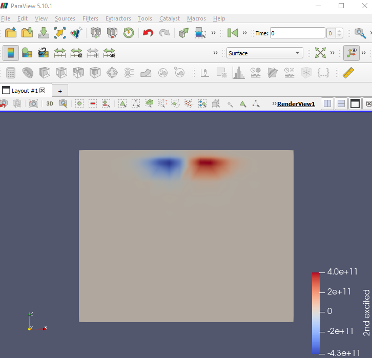
Fig. 2.5.5 Second excited state
2.6. Full code
__copyright__ = "Copyright 2022-2025, Nanoacademic Technologies Inc."

from qtcad.device import constants as ct
from qtcad.device.mesh3d import Mesh, SubMesh
from qtcad.device import io
from qtcad.device import materials as mt
from qtcad.device import Device, SubDevice
from qtcad.device.poisson import Solver as PoissonSolver
from qtcad.device.poisson import SolverParams as PoissonSolverParams
from qtcad.device.schrodinger import Solver as SchrodingerSolver
from qtcad.device import analysis as an
import pathlib

# Input file
script_dir = pathlib.Path(__file__).parent.resolve()
path_mesh = str(script_dir/'meshes'/'gated_dot.msh')

# Load the mesh
scaling = 1e-6
mesh = Mesh(scaling,path_mesh)
mesh.show()

# Create device
d = Device(mesh, conf_carriers="e")
d.set_temperature(0.1)

# Ionized dopant density
doping = 3e18*1e6   # In SI units

# Set up materials in heterostructure stack
d.new_region("cap", mt.GaAs)
d.new_region("barrier", mt.AlGaAs)
d.new_region("dopant_layer", mt.AlGaAs,ndoping=doping)
d.new_region("spacer_layer", mt.AlGaAs)
d.new_region("spacer_dot", mt.AlGaAs)
d.new_region("two_deg", mt.GaAs)
d.new_region("two_deg_dot", mt.GaAs)
d.new_region("substrate", mt.GaAs)
d.new_region("substrate_dot", mt.GaAs)

# Align the bands across hetero-interfaces using GaAs as the reference material
d.align_bands(mt.GaAs)

# Remove unphysical charge from cap and barrier
d.new_insulator("cap")
d.new_insulator("barrier")

# Applied potentials
Vtop_1 = -0.5
Vtop_2 = -0.5
Vtop_3 = -0.5
Vbottom_1 = -0.5
Vbottom_2 = -0.5
Vbottom_3 = -0.5

# Work function of the metallic gates at midgap of GaAs
barrier = 0.834*ct.e    # n-type Schottky barrier height

# Set up boundary conditions
d.new_schottky_bnd("top_gate_1", Vtop_1, barrier)
d.new_schottky_bnd("top_gate_2", Vtop_2, barrier)
d.new_schottky_bnd("top_gate_3", Vtop_3, barrier)
d.new_schottky_bnd("bottom_gate_1", Vbottom_1, barrier)
d.new_schottky_bnd("bottom_gate_2", Vbottom_2, barrier)
d.new_schottky_bnd("bottom_gate_3", Vbottom_3, barrier)
d.new_ohmic_bnd("ohmic_bnd")

# Create the non-linear Poisson solver and set its parameters
solver_params = PoissonSolverParams({"tol": 1e-3, "maxiter": 100})
poisson_solver = PoissonSolver(d, solver_params=solver_params)

# Create a submesh including only the dot region
submesh = SubMesh(mesh, ["spacer_dot","two_deg_dot","substrate_dot"])
submesh.show()

# Set up the dot region in which no classical charge is allowed
d.set_dot_region(submesh)

# Solve
poisson_solver.solve()

# Save the conduction band edge in .vtu format
outfile_cond_band_edge = str(script_dir / "output" / "cond_band_edge.vtu")
out_dict = {"EC (eV)": d.cond_band_edge()/ct.e}
io.save(outfile_cond_band_edge, out_dict, mesh)

# Save the electron density in .vtu format
outfile_electron_dens = str(script_dir / "output" / "electron_dens.vtu")
out_dict = {"n (1/m^3)": d.n}
io.save(outfile_electron_dens, out_dict, mesh)

# Get the potential energy from the band edge for usage in the Schrodinger
# solver
d.set_V_from_phi()

# Create a subdevice for the dot region
subdevice = SubDevice(d,submesh)

# Create a Schrodinger solver
schrod_solver = SchrodingerSolver(subdevice)

# Solve Schrodinger's equation
schrod_solver.solve()

# Print energies
subdevice.print_energies()

# Get and print the quantum-dot geometric properties
dot_props = an.analyze_dot(subdevice, verbose=True)

# Save the first few eigenstates
outfile_eigenfunctions = str(script_dir / "output" / "eigenfunctions.vtu")
out_dict = {"Ground": subdevice.eigenfunctions[:,0],
    "1st excited": subdevice.eigenfunctions[:,1],
    "2nd excited": subdevice.eigenfunctions[:,2]}
io.save(outfile_eigenfunctions, out_dict, submesh)