Band offset tutorial
Requirements
Software components
nanotools
RESCU+
ASE
Pseudopotentials
I will need the following pseudopotentials.
pseudos/band_alignment/Al_DZDP.mat
pseudos/band_alignment/As_DZP.mat
pseudos/band_alignment/Ga_DZP.mat
Let’s copy them from the pseudo database to the current working directory and export RESCUPLUS_PSEUDO=$PWD.
References
Dandrea, R. G. (1992). Interfacial atomic structure and band offsets at semiconductor heterojunctions. Journal of Vacuum Science & Technology B: Microelectronics and Nanometer Structures, 10(4), 1744.
Ask Hjorth Larsen, et al., The Atomic Simulation Environment—A Python library for working with atoms, J. Phys.: Condens. Matter Vol. 29 273002, 2017
Briefing
In this tutorial, I explain how to calculate the band offsets at a GaAs/AlAs interface.
Explanations
The calculations are summarized in the following figure from Dandrea et al.
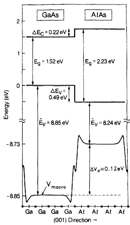
The macroscopic potential (\(V_{macro}\)) is the necessary heterostructure property. It is essentially an averaged version of the effective potential. It should recover it’s bulk value near the center of each material composing the heterostructure. One can then use it to position the valence band maximum (\(\tilde E_V\)) of each material, a quantity obtainable from bulk calcualtions. The conduction band minimum are obtained by using the experimental values of the band gaps. One can then readily derive the valence and conduction band offsets (\(\Delta E_V\) and \(\Delta E_C\))
I shall go through the following steps:
Accuracy check for AlAs and GaAs.
Calculation of the lattice parameter (a) of zinc-blende AlAs and GaAs.
Calculation of the lattice parameter (c) of tetragonal AlAs and GaAs under epitaxial constaints.
Calculation of the valence band maximum (\(\tilde E_V\)) with respect to the macroscopic potential in tetragonal GaAs and AlAs.
Calculation of the macroscopic potential (\(V_{macro}\)) in the relaxed heterostructure.
Put everything together and calculate the band offsets.
Accuracy control
In this section, I converge the total energy of AlAs and GaAs with respect to resolution and k-sampling. I shall only present the scripts briefly, for more details read this tutorial. I begin with executing the following Python script for AlAs.
from nanotools import Atoms, Cell, System, TotalEnergy
from nanotools.checkconv import CheckPrecision
a = 5.7
b = a / 2.
cell = Cell(avec=[[0.,b,b],[b,0.,b],[b,b, 0.]], resolution=0.20)
fxyz = [[0.  , 0.  , 0.  ],[0.25, 0.25, 0.25]]
atoms = Atoms(fractional_positions=fxyz, formula="AlAs")
sys = System(cell=cell, atoms=atoms)
ecalc = TotalEnergy(sys)
ecalc.solver.set_mpi_command("mpiexec --bind-to core -n 16")
ecalc.solver.set_stdout("resculog.out")
calc = CheckPrecision(ecalc, parameter="resolution", etol=1.e-3)
calc.solve()
The script for GaAs is the same except that
a = 5.6
atoms = Atoms(fractional_positions=fxyz, formula="GaAs")
A resolution of 0.12 Ang yields a total energy error of less than 1 meV per atom for both materials.
I then use that resolution in both materials and setup a k-sampling convergence object changing CheckPrecision as follows
calc = CheckPrecision(ecalc, parameter="k-sampling", etol=1.e-3)
to find a k-sampling of \(8\times 8\times 8\).
Lattice constants
In this section, I show how to obtain the lattice constant of AlAs and GaAs.
I use the EquationOfStates calculator to do so.
For more details on the EquationOfStates calculator, read this tutorial.
The following script sets up 5 calculations for primitive cells of varying volumes.
from nanotools import Atoms, Cell, System, TotalEnergy
from nanotools.eos import EquationOfState as EOS
import numpy as np
a = 5.7
b = a / 2.
cell = Cell(avec=[[0.,b,b],[b,0.,b],[b,b, 0.]], resolution=0.12)
fxyz = [[0.  , 0.  , 0.  ],[0.25, 0.25, 0.25]]
atoms = Atoms(fractional_positions=fxyz, formula="AlAs")
sys = System(cell=cell, atoms=atoms)
sys.kpoint.set_grid([8,8,8])
ecalc = TotalEnergy(sys)
ecalc.solver.set_mpi_command("mpiexec --bind-to core -n 16")
ecalc.solver.set_stdout("resculog.out")
calc = EOS.from_totalenergy(ecalc, relative_volumes=np.linspace(0.9,1.1,5))
calc.solve()
Once the calculations are completed, I use the plot_eos function to show an equation of state fit to the energy and volume data (per atom).
from nanotools.eos import EquationOfState as EOS
calc = EOS.read("nano_eos_out.json")
calc.plot_eos(filename='AlAs-eos.png', show=False)
It will show the following
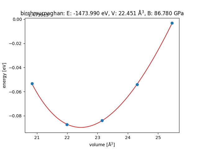
This gives me the equilibrium volume of the FCC primitive cell. To get the equilibrium lattice constant, I multiply by 2 (atoms) and by 4, the FCC to CUB factor, and take the cubic root. I obtain 5.642 Ang.
Repeating the procedure for GaAs I find a lattice parameter of 5.588 Ang.
Epitaxial lattice constants
In this section, I show how to obtain the lattice constant of epitaxial AlAs and GaAs under epitaxial constraint. In the previous sections, I found the lattice constant of AlAs to be 5.642 Ang and that of GaAs to be 5.588 Ang. Down the line, I will calculate the band offsets for the (001) interface between AlAs and GaAs. I now make the assumption that each material will take roughly 50% of the strain, which means that the heterojunction will have a lattice constant of 5.615 = (5.642 + 5.588) / 2 Ang in the x- and y-directions. The stress will dissipate in the z-direction resulting in a tetragonal geometry. I will thus recalculate the lattice constant of AlAs in the z-direction using a cubic fit. The following script sets up 5 calculations for tetragonal cells of varying lengths.
from nanotools import Atoms, Cell, System, TotalEnergy
import numpy as np
a = 5.615
b = a / np.sqrt(2)
fxyz = [[0.  , 0.  , 0.  ],[0.5 , 0.  , 0.25],
       [0.5 , 0.5 , 0.5 ],[0.  , 0.5 , 0.75]]
atoms = Atoms(fractional_positions=fxyz, formula="AlAsAlAs")
cell = Cell(avec=np.diag([b,b,a]), resolution=0.12)
sys = System(cell=cell, atoms=atoms)
sys.kpoint.set_grid([8,8,6])
ecalc = TotalEnergy(sys)
ecalc.solver.set_mpi_command("mpiexec --bind-to core -n 16")
ecalc.solver.set_stdout("resculog.out")
vols = []; etots = []; n = 0
for f in np.linspace(0.9,1.1,5):
   cell = Cell(avec=np.diag([b,b,a*f]), resolution=0.12)
   ecalc.system.set_cell(cell)
   ecalc.solver.restart.clear_paths()
   ecalc.solve(output=f"nano_scf_out_{n}")
   vols.append(a*f)
   etots.append(ecalc.get_total_energy_per_atom().m)
   np.savez("data",vols=vols,etots=etots)
   n += 1
The energy and volume data is saved to data.npz as it is computed.
I then use numpy to perform a cubic fit to get the equilibrium lattice constant: 5.674 Ang.
For GaAs, the same procedure yields: 5.574 Ang
Valence band edge of GaAs
I now seek the position of the valence band edge (\(\tilde{E_V}\)) of AlAs and GaAs with respect to the macroscopic potential (\(V_{macro}\)).
This is a bulk property which I obtain from a band structure calculation of the tetragonal cell.
For detailed instructions regarding band structure calculations, refer to tutorial_bs.md.
I use the following script to get the ground state potential and band structure of AlAs.
import numpy as np
from nanotools import Atoms, Cell, System, TotalEnergy
from nanotools.bandstructure import BandStructure as BS
a = 5.615
b = a / np.sqrt(2)
c = 5.674
fxyz = [[0.  , 0.  , 0.  ],[0.5 , 0.  , 0.25],
       [0.5 , 0.5 , 0.5 ],[0.  , 0.5 , 0.75]]
atoms = Atoms(fractional_positions=fxyz, formula="AlAsAlAs")
cell = Cell(avec=np.diag([b,b,c]), resolution=0.12)
sys = System(cell=cell, atoms=atoms)
sys.kpoint.set_grid([8,8,6])
ecalc = TotalEnergy(sys)
ecalc.solver.set_mpi_command("mpiexec --bind-to core -n 16")
ecalc.solver.set_stdout("resculog.out")
ecalc.solve()
bcalc = BS.from_totalenergy(ecalc)
bcalc.solve()
I now locate the valence band edge with respect to the macroscopic potential.
from nanotools import TotalEnergy, BandStructure as BS
import numpy as np
ecalc = TotalEnergy.read("nano_scf_out.json")
bcalc = BS.read("nano_bs_out.json")
veff = ecalc.get_field("potential/effective")
vmac = np.mean(veff)
vbm = bcalc.energy.get_vbm()
print("%20s = %f" % ("vmacro (eV)", vmac.m))
print("%20s = %f" % ("vbm (eV)", vbm.m))
print("%20s = %f" % ("vbm - vmacro (eV)", vbm.m - vmac.m))
I read the ground state results using TotalEnergy.read and load the effective potential (\(v_{pp} + v_H + v_{xc}\)) using the get_field function.
The units are automatically converted from Hartree (in the HDF5 file) to eV.
Next, I use the Energy class method get_vbm which returns the maximal eigenvalue under the Fermi level.
Finally I print the information to screen and get
         vmacro (eV) = -20.098377
            vbm (eV) = -6.625077
   vbm - vmacro (eV) = 13.473300
The same procedure for GaAs yields
         vmacro (eV) = -20.566220
            vbm (eV) = -6.022645
   vbm - vmacro (eV) = 14.543575
Relaxation of the heterostructure
In this section, I build and relax the heterostructure. When the two materials come into contact, they will exchange electrons near the interface, leading the a so-called interface dipole. The charge transfer induces interface-localized stress, which leads to non-negligible forces on the atoms near the interface. Relaxation of the atoms usually result in an additional dipole which must be taken into account in the band alignment. I thus build and relax the heterostructure as follows.
from ase.build import bulk, stack, make_supercell
from ase.optimize import BFGS
from nanotools.ext.calculators.ase import Rescuplus
import numpy as np
import os

a = 5.615
c = 5.674
alas = bulk('AlAs', crystalstructure='zincblende', a=a, orthorhombic=True)
alas.set_cell(alas.cell * np.array([1.,1.,c/a]), scale_atoms=True)
alas = make_supercell(alas, [[1,0,0],[0,1,0],[0,0,4]])
alas.center()

a = 5.615
c = 5.574
gaas = bulk('GaAs', crystalstructure='zincblende', a=a, orthorhombic=True)
gaas.set_cell(gaas.cell * np.array([1.,1.,c/a]), scale_atoms=True)
gaas = make_supercell(gaas, [[1,0,0],[0,1,0],[0,0,4]])
gaas.center()

slab = stack(alas, gaas)

inp = {}
inp["system"] = { "cell" : {"resolution": 0.12}, "kpoint" : {"grid":[8,8,1]}}
inp["solver"] = {"mix": {"metric": "ker", "precond": "ker"}}
inp["solver"]["eig"] = {"lwork" : 2**24, "algo" : "mrrr"}
inp["solver"]["restart"] = {"DMkPath": "nano_scf_out.h5"}
inp["energy"] = {"forces_return": True}
mpicmd = "mpiexec -n 36 "
rsccmd = mpicmd+" rescuplus -i PREFIX.rsi && mv nano_scf_out.json PREFIX.rso"
calc = Rescuplus(command=rsccmd, input_data=inp)
slab.calc = calc

os.system("rm -f nano_scf_out.h5")
opt = BFGS(slab, trajectory="hetero.traj", logfile="relax.out")
opt.run(fmax=0.01)
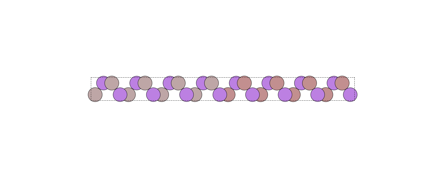
I create two \(1 \times 1 \times 4\) supercells from the tetragonal cells of GaAs and AlAs (orthorhombic option), then stack them using the stack function of ase.build.
I then get a 32-monolayer heterostructure which I can visualize using the view function of the ase.visualize module.
 I also set
 solver.restart.DMRPath to nano_scf_out.h5 to employ real space density matrix restart during the relaxation procedure.
This will typically save at least a few self-consistent iterations in the computation of the ground state of each atomic configuration.
Atomic relaxation is usually most significant within the first one to three monolayers.
However, one should be careful to converge his results with respect to heterostructure thickness.
During the relaxation, the atomic configurations are saved to hetero.traj, as commanded by the parameter trajectory of the BFGS solver.
You can visualize the relaxation process typing
ase gui hetero.traj
You may think that atoms move very slightly, but the effect on the interface dipole is actually significant.
Band diagram of the heterostructure
In this section, I create the band diagram from the results obtained in the previous sections. I first concentrate on massaging the effective potential of the heterostructure into the macroscopic potential (\(V_{macro}\)). I first obtain the average potential (\(V_{avg}\)) by taking the average in the directions transverse to the heterostructure (here the x- and y-directions).
from nanotools import TotalEnergy
ecalc = TotalEnergy.read("nano_scf_out.json")
fig = ecalc.plot_field("potential/effective", axis=2, filename="band_diagram.png")
I begin by reading the results with TotalEnergy.read.
Then I plot the effective potential \(V_{avg}\) along the z-direction (axis=2) using the method plot_field.
You should get the following plot.
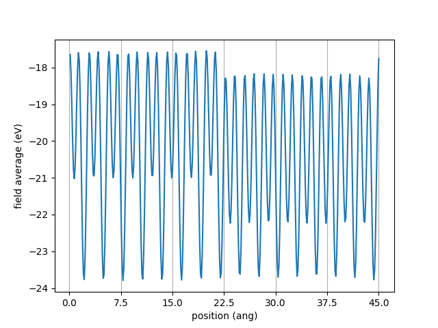
It is difficult to align the valence bands on the averaged potential since it still shows large oscillations due to the atomic potentials.
I thus use smooth_field which will smooth the average field by convolution with an erf pulse.
import os
os.chdir("/home/vincentm/repos/1-rescuf08/examples/band_offset/relax")
from nanotools import TotalEnergy
ecalc = TotalEnergy.read("nano_scf_out.json")
veff = ecalc.smooth_field("potential/effective", axis=2)
fig = ecalc.plot_field(veff, axis=2)
I then get a figure like
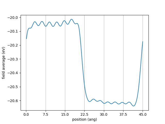 It is now apparent that the macroscopic potential reaches some bulk value in each material away from the interfaces.
It is those values that I use to align the valence band minimum (using \(\tilde E_V\) calculated above).
It is now apparent that the macroscopic potential reaches some bulk value in each material away from the interfaces.
It is those values that I use to align the valence band minimum (using \(\tilde E_V\) calculated above).
The final step is to summarize everything in a figure and calculate the band offsets.
This is done by the following Python script (assuming vmac is defined as in the above script).
import numpy as np
import matplotlib.pyplot as plt
from nanotools import TotalEnergy
ecalc = TotalEnergy.read("nano_scf_out.json")
vmac = ecalc.smooth_field("potential/effective", axis=2)
z = ecalc.system.cell.get_grid(axis=2)
lz = ecalc.system.cell.get_length(axis=2)

# vmacro-alas
gapa = 2.23
ca = 5.674; lima = np.array([ca, 3*ca])
vmac_alas = np.mean(vmac[np.logical_and(z.m > lima[0], z.m < lima[1])])
vbm_alas = vmac_alas.m + 13.473300
cbm_alas = vbm_alas + gapa
# vmacro-gaas
gapb = 1.52
cb = 5.574; limb = np.array([cb, 3*cb]) + 4*ca
vmac_gaas = np.mean(vmac[np.logical_and(z.m > limb[0], z.m < limb[1])])
vbm_gaas = vmac_gaas.m + 14.543575
cbm_gaas = vbm_gaas + gapb
# offsets
vbm_off = vbm_gaas - vbm_alas
cbm_off = -(cbm_gaas - cbm_alas)
print("vbm offset (+gaas higher): %f (eV)" % vbm_off)
print("cbm offset (+alas higher): %f (eV)" % cbm_off)
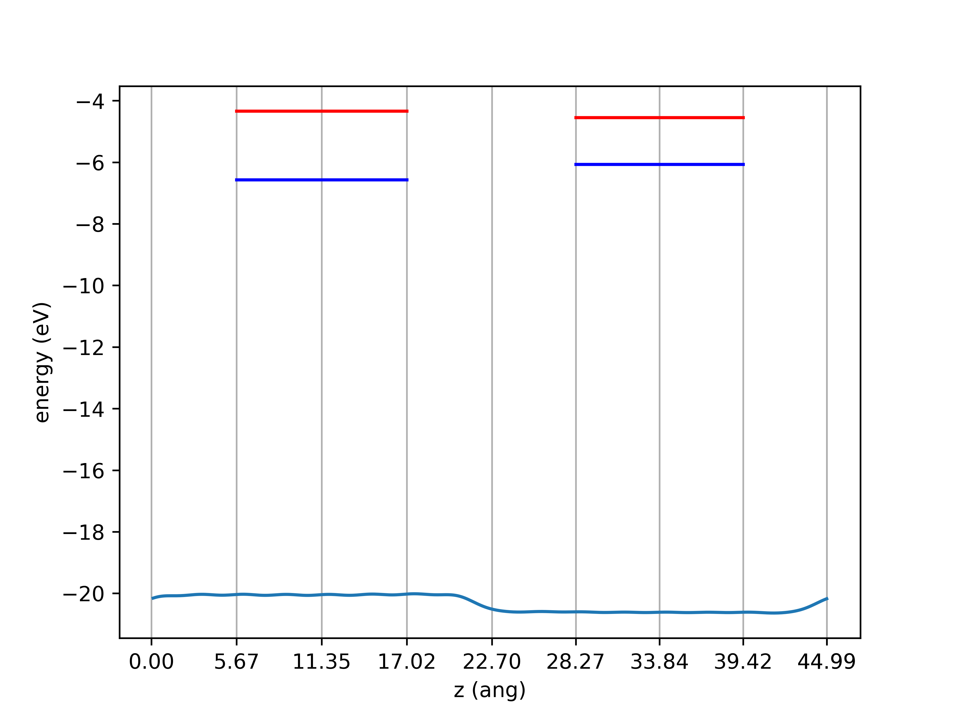
There are still some wiggles in the macroscopic potential, but I need one number for each material. I thus average the macroscopic potential over the two central unit cells. I then add the valence band maxima to the macroscopic potentials and subtract them to obtain the valence band offsets. The conduction band offsets are obtained by adding the experimental gap values to the valence band maxima and subtracting again. I finally find
vbm offset (+gaas higher): 0.499948 (eV)
cbm offset (+alas higher): 0.210052 (eV)
The valence band offset is about 50 meV smaller than the experimental value of 0.55 eV. The conduction band offset on the other hand is identical at 0.20 eV. This is partly luck as I have neglected many effects (e.g. spin-orbit coupling). But you can now go through the band alignment steps by yourself for various material combinations.
The band diagram may be plotted as follows
fig = plt.figure()
plt.plot(z.m, vmac.m, label='vmacro')
plt.plot(lima, np.ones(2)*(vbm_alas), 'b', label='vbm_alas')
plt.plot(lima, np.ones(2)*(cbm_alas), 'r', label='cbm_alas')
plt.plot(limb, np.ones(2)*(vbm_gaas), 'b', label='vbm_gaas')
plt.plot(limb, np.ones(2)*(cbm_gaas), 'r', label='cbm_gaas')
plt.xticks([0, ca, 2*ca, 3*ca, 4*ca, cb+4*ca, 2*cb+4*ca, 3*cb+4*ca, 4*cb+4*ca, lz.m])
plt.grid(axis='x')
plt.xlabel("z (ang)")
plt.ylabel("energy (eV)")
plt.show()
fig.savefig("hetero_gaas_alas_diag.png", dpi=600)
which looks as follows