Defect project tutorial
Requirements
Software components
nanotools
RESCU+
ASE
Pseudopotentials
I will need the following pseudopotential file:
C_SZDP.mat
Let’s copy it from the pseudo database to the current working directory and export RESCUPLUS_PSEUDO=$PWD.
References
Freysoldt, C., Neugebauer, J., & Van De Walle, C. G. (2009). Fully Ab initio finite-size corrections for charged-defect supercell calculations. Physical Review Letters, 102(1), 016402.
Freysoldt, C., Neugebauer, J., & Van de Walle, C. G. (2011). Electrostatic interactions between charged defects in supercells. Physica Status Solidi (B) Basic Research, 248(5), 1067–1076.
Freysoldt, C., Grabowski, B., Hickel, T., Neugebauer, J., Kresse, G., Janotti, A., & Van De Walle, C. G. (2014). First-principles calculations for point defects in solids. Reviews of Modern Physics, 86(1), 253–305.
Kumagai, Y., & Oba, F. (2014). Electrostatics-based finite-size corrections for first-principles point defect calculations. Physical Review B, 89(19), 195205.
Ask Hjorth Larsen, et al., The Atomic Simulation Environment—A Python library for working with atoms, J. Phys.: Condens. Matter Vol. 29 273002, 2017
Briefing
In this tutorial, I explain how to calculate the defect level diagram of a carbon vacancy in diamond.
Explanations
I will calculate the formation energy as a function of chemical potential of several charge states of the defect. The formation energy of a charged defect is given by
where \(E[D^q]\) is the total energy of the defect system with charge q, \(E[Host]\) is the total energy of the perfect system, \(n_s\) is the number of atoms of species \(s\) added (if positive) or removed (if negative). For instance, in the diamond vacancy, we have \(n_C = -1\). \(\mu_s\) is the chemical potential of species \(s\), \(E^{Fermi}\) is the chemical potential of the electrons and \(E_{corr}(q,\epsilon)\) is a correction that account for finite size effects. I will use the correction scheme of Kumagai and Oba, which requires determining the dielectric constant of diamond.
After obtaining the defect formation energies of several charge states, we can compute the following transition level diagram
I shall go through the following steps:
Determine values for the accuracy parameters.
Determine the equilibrium structure.
Compute the atomic chemical potential.
Compute the electronic chemical potential.
Compute the dielectric tensor.
Setup a defect calculator.
Analyze the neutral defect band structure.
Get the charged defect formation energy.
Plot the transition level diagram.
Accuracy parameters
In this section, I converge the total energy of a diamond conventional unit cell with respect to resolution and k-sampling.
To begin with, I define the xyz file diamond.fxyz
8
# diamond
C   0.0000   0.0000   0.0000
C   0.0000   0.5000   0.5000
C   0.5000   0.0000   0.5000
C   0.5000   0.5000   0.0000
C   0.2500   0.2500   0.2500
C   0.2500   0.7500   0.7500
C   0.7500   0.2500   0.7500
C   0.7500   0.7500   0.2500
with the fractional coordinates of a conventional cell of a diamond crystal.
I now follow the procedure described in the tutorial on accuracy.
I initialize a System object for a diamond crystal with lattice constant 3.56 Ang and resolution 0.2 Ang.
from nanotools import Atoms, Cell, System, TotalEnergy
from nanotools.checkconv import CheckPrecision
a = 3.56
cell = Cell(avec=[[a,0.,0.],[0.,a,0.],[0.,0.,a]], resolution=0.20)
atoms = Atoms(fractional_positions="diamond.fxyz")
sys = System(cell=cell, atoms=atoms)
ecalc = TotalEnergy(sys)
ecalc.solver.set_mpi_command("mpiexec -n 16")
ecalc.solver.set_stdout("resculog.out")
calc = CheckPrecision(ecalc, parameter="resolution", etol=1.e-3)
calc.solve()
These values need only be reasonable guesses at this point. The output is as follows
    resolution (ang) |    total energy (ev) |    energy error (ev)
          0.20000000 |       -1311.11053244 |          +0.01480684
          0.18000000 |       -1311.14730487 |          -0.02196559
          0.16200000 |       -1311.12141341 |          +0.00392587
          0.14580000 |       -1311.12704976 |          -0.00171048
          0.13122000 |       -1311.11882914 |          +0.00651014
          0.11809800 |       -1311.12641615 |          -0.00107686
          0.10628820 |       -1311.12459908 |          +0.00074020
          0.09565938 |       -1311.12602159 |          -0.00068230
          0.08609344 |       -1311.12533928 |          +0.00000000
I need not be terribly precise for this tutorial, so I’ll set the resolution to 0.15 Ang.
I then setup a CheckPrecision calculator to determine a k-sampling.
from nanotools import Atoms, Cell, System, TotalEnergy
from nanotools.checkconv import CheckPrecision
a = 3.56
cell = Cell(avec=[[a,0.,0.],[0.,a,0.],[0.,0.,a]], resolution=0.15)
atoms = Atoms(fractional_positions="diamond.fxyz")
sys = System(cell=cell, atoms=atoms)
ecalc = TotalEnergy(sys)
ecalc.system.kpoint.set_grid([3,3,3])
calc = CheckPrecision(ecalc, parameter="k-sampling", etol=1.e-3)
calc.solve()
The output is as follows
          k-sampling |    total energy (ev) |    energy error (ev)
     3      3      3 |       -1311.07886651 |          +0.06439917
     4      4      4 |       -1311.14418666 |          -0.00092099
     5      5      5 |       -1311.14326568 |          +0.00000000
I’ll set the k-sampling grid to [5,5,5].
Equilibrium structure
In this section, I show how to obtain the equilibrium structure of diamond. There are several ways to do so:
Equation of states;
Quadratic fit;
Fully relaxing the system’s cell and atomic coordinates.
I will use nanotools’s equation of state class to derive the equilibrium structure, since we already know the fractional coordinates of the diamond ground state. I only need to find one lattice parameter. Following the EOS tutorial, I sets up 5 calculations of unit cells of varying volumes.
from nanotools import Atoms, Cell, System, TotalEnergy
from nanotools.eos import EquationOfState as EOS
import numpy as np
a = 3.56
cell = Cell(avec=[[a,0.,0.],[0.,a,0.],[0.,0.,a]], resolution=0.15)
atoms = Atoms(fractional_positions="diamond.fxyz")
sys = System(cell=cell, atoms=atoms)
sys.kpoint.set_grid([5,5,5])
ecalc = TotalEnergy(sys)
eos = EOS.from_totalenergy(ecalc)
eos.relative_volumes = np.linspace(0.95, 1.05, 5)
eos.solve()
eos.plot_eos(filename="eos.png")
I read the data and find an equilibrium volume per atom of
>>> from nanotools.eos import EquationOfState as EOS
>>> calc = EOS.read("nano_eos_out.json")
>>> v0=calc.get_equilibrium_volume()
>>> print(f"Equilibrium volume = {v0}")
Equilibrium volume = 5.642033273026279
The lattice constant is obtained multiplying by 8 (atoms) and taking the cubic root, which gives 3.56048 Ang.
I will simply round it to 3.560 Ang.
Let’s now define the following TotalEnergy calculator and save it to nano_scf_ref.json for reference.
from nanotools import Atoms, Cell, System, TotalEnergy
a = 3.560
cell = Cell(avec=[[a,0.,0.],[0.,a,0.],[0.,0.,a]], resolution=0.15)
atoms = Atoms(fractional_positions="diamond.fxyz")
sys = System(cell=cell, atoms=atoms)
sys.kpoint.set_grid([5,5,5])
ecalc = TotalEnergy(sys)
ecalc.write("nano_scf_ref.json")
Atomic chemical potential
In this section, I show how to obtain the atomic chemical potential of diamond.
The elemental chemical potential generally depends on experimental conditions. In theoretical work, one usually uses elemental crystal phases as a reference, simulating atoms being exchanged with a particle bath consisting of the elemental crystal. In general, one should go through the following steps for each atomic species involved:
Find the most stable elemental phase.
Find the equilibrium cell shape and atomic positions.
Compute the total energy per atom for the lowest energy configuration.
Here, the chemical potential is simply the total energy per atom of the pure diamond crystal and we may skip to the last step.
from nanotools import TotalEnergy
calc = TotalEnergy.read("nano_scf_ref.json")
calc.solve()
print("Total energy per atom = %f %s" % (calc.get_total_energy_per_atom().m, calc.get_total_energy_per_atom().u))
I obtain
Total energy per atom = -163.892908 ev
Electronic chemical potential
In this section, I show how to obtain the electronic chemical potential of diamond or Fermi energy.
In theoretical work, one usually references the Fermi energy to the valence band maximum of the perfect host crystal.
I will obtain this value using a ValenceBandMaximum calculator as explained in this tutorial.
I will use \(\delta N = 10^{-3}\) which is usually a good value, but one should really try several values, more or less small.
I thus need to do at least two calculations, one for the neutral unit cell and one for the slightly charged unit cell.
nanotools can do that for you
from nanotools.vbm import ValenceBandMaximum as VBM
from nanotools.totalenergy import TotalEnergy
calc = VBM.from_totalenergy("nano_scf_ref.json")
calc.delta_charges = [0.001]
calc.solve()
vbm = calc.get_vbm()
print(f"The VBMs are = {vbm}")
I get the following output
The VBM is = 10.119736 ev
Dielectric tensor
The correction term for charged defect state depends on the dielectric tensor of the material.
One should compute and employ the theoretical values for consistency.
The dielectric tensor is symmetric and satisfies the symmetry of the crystal.
In diamond, there is therefore a single number to compute \(\epsilon_{11}\) since \(\epsilon_{11} = \epsilon_{22} = \epsilon_{33}\).
The off-diagonal elements are zero.
I will obtain this value using a DielectricConstant calculator as explained in this tutorial.
I use a \(1\times 1 \times 4\) supercell and a sawtooth potential with an amplitude of 0.1 eV along the z-direction.
from nanotools import TotalEnergy
from nanotools.dielectric import DielectricConstant
ecalc = TotalEnergy.read("nano_scf_ref.json")
ecalc.supercell([1,1,4])
ecalc.system.kpoint.set_grid([5,5,1])
calc = DielectricConstant(ecalc, axis=2, amplitude=0.1)
calc.solve()
print("eps11 = %f" % (calc.get_dielectric_constant()))
I get a dielectric constant of
eps11 = 5.352788
Setup a defect project
I use the Defect class to create a defect project.
import numpy as np
from nanotools.defect import Defect
from nanotools.totalenergy import TotalEnergy
ecalc = TotalEnergy.read("nano_scf_ref.json")
d = Defect(name="vac", unitsys=ecalc, supercell=[2,2,2], charges=list(range(-4,3)), site=0)
d.chemicalpotentials({"C": -163.889935})
d.efermi(10.097401)
d.dielectric(5.359590 * np.eye(3))
d.bandgap(5.47)
d.relax = False
d.write("dvac.json")
d.create_directories()
d.solve()
Calling create_directories will create the directory vac (according to the attribute name).
All calculations will be done in there.
It also creates a rigid directory structure that RESCU+ relies on to lookup and combine results from various calculations.
The directory structure will look like
vac/
├── natm_64
    ├── defect_q0
    ├── defect_qm1
    ├── defect_qm2
    ├── defect_qm3
    ├── defect_qm4
    ├── defect_qp1
    ├── defect_qp2
    └── host
The top level directory contains some reference files like the JSON of the TotalEnergy calculator.
The other directories are created to perform calculations and hold results.
Neutral defect band structure
In this section, I compute the band structure of the neutral vacancy in diamond. This is to give myself an idea of the electronic structure of the defect, which will determine how I do things next. As we shall see, the diamond vacancy has a six-fold degenerate defect state (including spin degeneracy). This leads to a finite size effect: the artificial dispersion of the defect levels across the Brillouin zone. This so-called band dispersion error is mitigated using a uniform occupation scheme instead of, say, Fermi-Dirac occupancies.
So we need to know the band structure enough to know how to populate it. Let’s compute the band structure of a 64 atom supercell, which should be enough for this kind of spadework.
import numpy as np
from nanotools import TotalEnergy
calc = TotalEnergy.read("../../nano_scf_ref.json")
calc.supercell(T=np.diag([2,2,2]))
calc.system.vacate(site=0)
calc.solve()
I used the supercell method to create a supercell of the system within the TotalEnergy object.
I also use the vacate method to create a vacancy at the 0-site.
The previous step will also introduce a vacancy atom at the 0-site, i.e. one without pseudopotential, but with the original atomic orbital basis.
Also, when calling solve, the output should be left as nano_scf_out.json, since Defect objects will look for those to parse results.
I then compute the band structure using
from nanotools import TotalEnergy, BandStructure as BS
ecalc = TotalEnergy.read("nano_scf_out.json")
calc = BS.from_totalenergy(ecalc)
calc.system.set_kpoint_path(special_points=["X","G","M"], grid=50)
calc.solve()
fig = calc.plot_bs(filename="bs.png")
I then plot the band structure to see what is going on and get something like
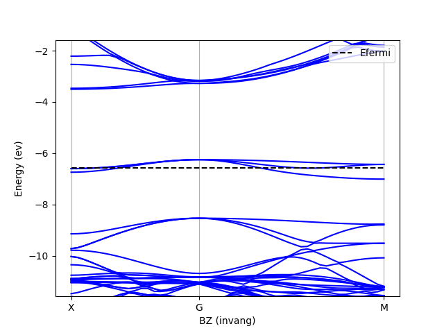
The Fermi level goes through the defect levels, which have a significant dispersion as expected. To minimize finite-size effects, I will populate these levels uniformly with 1/3 of a electron.
Neutral formation energy
Now that I know the electronic structure, I’m ready to perform the final supercell calculation.
I jump to natm_64/defect_q0 and open the following file.
import numpy as np
from nanotools import TotalEnergy
calc = TotalEnergy.read("../../nano_scf_ref.json")
calc.supercell(T=np.diag([2,2,2]))
calc.system.vacate(site=0)
nval = calc.system.atoms.valence_charge
calc.system.set_occ(bands = [nval/2, nval/2 + 2], occ=2.000000/6.)
calc.solve()
The script is first creating a \(2\times 2\times 2\) supercell and vacating the 0-site as before.
I set the occupancy of the defect bands (indexed [nval/2, nval/2 + 2]) to one third.
The bands under nval/2 are assumed to be completely filled and those above nval/2 + 2 completely empty.
It then changes the population scheme to "fixed" and adjust the total valence charge in the system.
Again, when calling solve, the output should be left as nano_scf_out.json, since Defect objects will look for those to parse results.
Charged defect formation energy
Charged defect supercell calculations are quite similar to the neutral defect one. For instance, the q = -2 input file looks like
import numpy as np
from nanotools import TotalEnergy
calc = TotalEnergy.read("../../nano_scf_ref.json")
calc.supercell(T=np.diag([2,2,2]))
calc.system.vacate(site=0)
nval = calc.system.atoms.valence_charge
calc.system.set_occ(bands = [nval/2, nval/2 + 2], occ=4.000000/6.)
calc.solve()
Note that I call set_occ(bands = [nval/2, nval/2 + 2], occ=4.000000/6.).
The valence charge will be augmented by 2 (electrons) and the occupation of the defect bands to 2/3 accordingly.
Finally the solve method of TotalEnergy is called to perform the calculation and save the results to nano_scf_out.json.
If all supercell scripts are properly set up, you can run all of them automatically calling a script like
from nanotools.defect import Defect
d = Defect.read("dvac.json")
d.solve()
at the root.
Once all calculations are done, here defect_q0, defect_qm1, defect_qm2, defect_qm3, defect_qm4, defect_qp1, defect_qp2 and host, the formation energies can be computed.
I compute the formation energies and electrostatic corrections as follows
from nanotools.defect import Defect
d = Defect.read("dvac.json")
d.get_formation_energies(correct=True)
print(d.formationenergies)
d.write("dvac.json")
and get
[ 7.78736436  7.5282134   8.40749712 10.59609682 14.19720808 19.21110798
 25.53669325]
I also saved the corrected formation energies calling the write method.
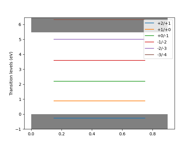
Transition level diagram
Once the corrected levels are obtained, the defect object may be inspected for further analysis.
The method plot_transition_level_diagram generates a plot of the transition level diagram.
from nanotools.defect import Defect
d = Defect.read("dvac.json")
d.get_transition_levels(correct=True)
fig = d.plot_transition_level_diagram(filename="tld.png")
This yields something like
In this tutorial, we used unrelaxed 64 atom supercells. In a scientific publication, the above steps should be repeated for bigger supercells (e.g. 216 atoms) to quantify finite-size effects. In many scientific problems, the relevant defect atomic configurations are not those of the perfect host crystal, but the relaxed atomic configurations. All defect supercells should therefore be relaxed. In this case, the relevant dielectric calculations are not static configuration response, but should also include atomic relaxation.