2. GaAs: band structure along the FCC path
Gallium arsenide is the classic III–V semiconductor, and its band structure is a two-step workflow: a self-consistent ground state, then eigenvalues along the standard high-symmetry path of the FCC Brillouin zone. This tutorial also demonstrates something subtler — how LatticeMind reports a result honestly when the level of theory is known to distort it.
What you need
The same setup as Silicon: SCF, band structure & DOS. Start to finish, this project runs in about three minutes on a laptop.
2.1. The prompt
This is one of the ready-to-run prompts shipped with /examples:
Create a two-step zinc-blende GaAs workflow: SCF with a saved density, then
a band structure along the standard FCC path.
2.2. What LatticeMind does
Plans
SCF→BAND-STRUCTURE, with the band step reading the converged density throughrho.in.Builds the two-atom zinc-blende cell (Ga at the origin, As at ¼¼¼).
Renders and validates both decks, then runs them.
Plots the bands along Γ–X–W–K–Γ–L–U–W–L–K — the standard FCC path, chosen from a fixed table for the detected lattice, with each label placed at its true position along the path.
2.3. The results
Quantity |
Value |
|---|---|
SCF total energy |
−78.4265 Ha |
Integrated electron count |
18.0 e |
Band gap (PBE) |
0.00 eV — flagged, see below |
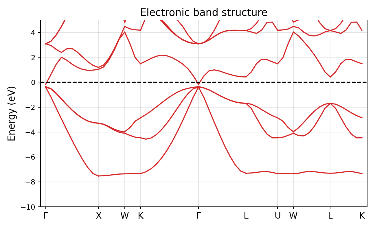
Fig. 2.3.1 Zinc-blende GaAs bands along Γ–X–W–K–Γ–L–U–W–L–K, generated from the converged SCF density. Note the unequal label spacing: each segment occupies its true share of the reciprocal-space path length.
2.4. An honest zero
Experimentally, GaAs has a direct gap of about 1.42 eV. Within PBE the gap collapses to zero — a well-known failure of semi-local functionals for small-gap semiconductors, more severe here than the ~50 % underestimate you saw for silicon.
What matters is how this is reported. LatticeMind does not call GaAs a
metal. The analysis records a structured warning naming the collapse as an
expected artifact of the functional, the report says a hybrid functional or
many-body correction is needed for a quantitative gap, and the extracted
band_gap = 0.0 is presented with that caveat attached. The honest answer
to “what is the PBE gap of GaAs?” is zero — and the report makes sure the
number cannot be mistaken for a physical prediction.
2.5. What you learned
The shipped
/examplesprompts are verified, copy-paste starting points.Band paths are deterministic: the FCC path and its labels come from the detected lattice, and the plot places every label at its exact vertex.
A known limitation of the level of theory is reported as one, not passed off as a physical result.
For the k-point convergence companion study, continue to Aluminium: a k-point convergence study.