2. NanoDCAL: electronic structure and transport
Note
The calculations here run on a local NanoDCAL installation or on an HPC cluster. For everything NanoDCAL can do, see NanoDCAL support; to continue a transport project across several requests, see Continuing a transport project.
LatticeMind’s NanoDCAL backend brings quantum-transport-oriented calculations into the same plain-language workflow. You select it simply by saying “Using NanoDCAL, …” in your prompt. This tutorial walks through a silicon band structure, then points to the full two-probe transport workflow.
2.1. Silicon band structure
Using NanoDCAL, run an SCF and band structure calculation for silicon.
LatticeMind builds the silicon crystal, stages the LCAO basis files with the project, runs the SCF, then computes the band structure along the standard high-symmetry path — and plots it referenced to the Fermi level:
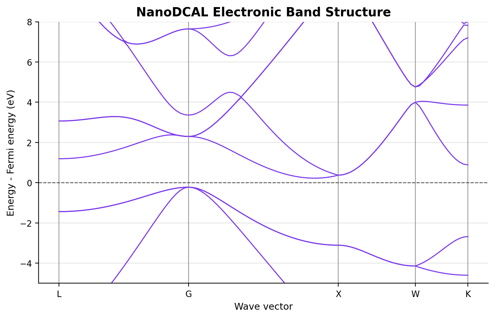
Fig. 2.1.1 Silicon band structure from NanoDCAL, along L–Γ–X–W–K with energies referenced to the Fermi level (dashed line). The indirect gap between the valence-band maximum at Γ and the conduction-band minimum near X is clearly resolved.
2.2. Validate the band-gap interpretation
The plotted zero is the NanoDCAL Fermi energy. The reported silicon gap is obtained from the occupied and unoccupied bands sampled along the full L–Γ–X–W–K path. It is therefore an indirect path-sampled gap, not the energy separation between two states selected at one k-point.
This distinction matters when comparing BandStructure.mat with
EigenStates.mat. For example, requesting one state below and one state above
the Fermi level on a [1, 1, 1] grid samples two Γ-point states. Their direct
separation can be much larger than silicon’s indirect band gap and should not
be reported as the PBE fundamental gap.
Before using the value in a manuscript:
repeat the SCF calculation with a denser k-grid and keep the plotted high-symmetry path unchanged;
record the exchange-correlation functional and NeutralAtomDatabase basis choice, because both affect the numerical gap;
confirm that
results/analysis_summary.jsonreports the same band edges visible in the figure; andremember that a converged PBE gap is a method-specific result, not an experimental-gap correction.
Tip
Because the LCAO basis travels with the project (nanodcal_basis/), the
generated project runs unchanged on another machine — locally or on a remote
NanoDCAL server (see Remote & HPC execution). When sharing the generated project,
please keep the staged NeutralAtomDatabase files within the scope of your
Nanoacademic license.
2.3. Spin-resolved transmission channels
This prompt exercises the transverse-k and spin dimensions in
TransmissionChannel.mat:
Using NanoDCAL, run SCF and transmission-channel analysis for
ferromagnetic bcc iron.
LatticeMind plots the channel count on the regular transverse-k mesh and keeps the spin-up and spin-down maps on the same colour scale:
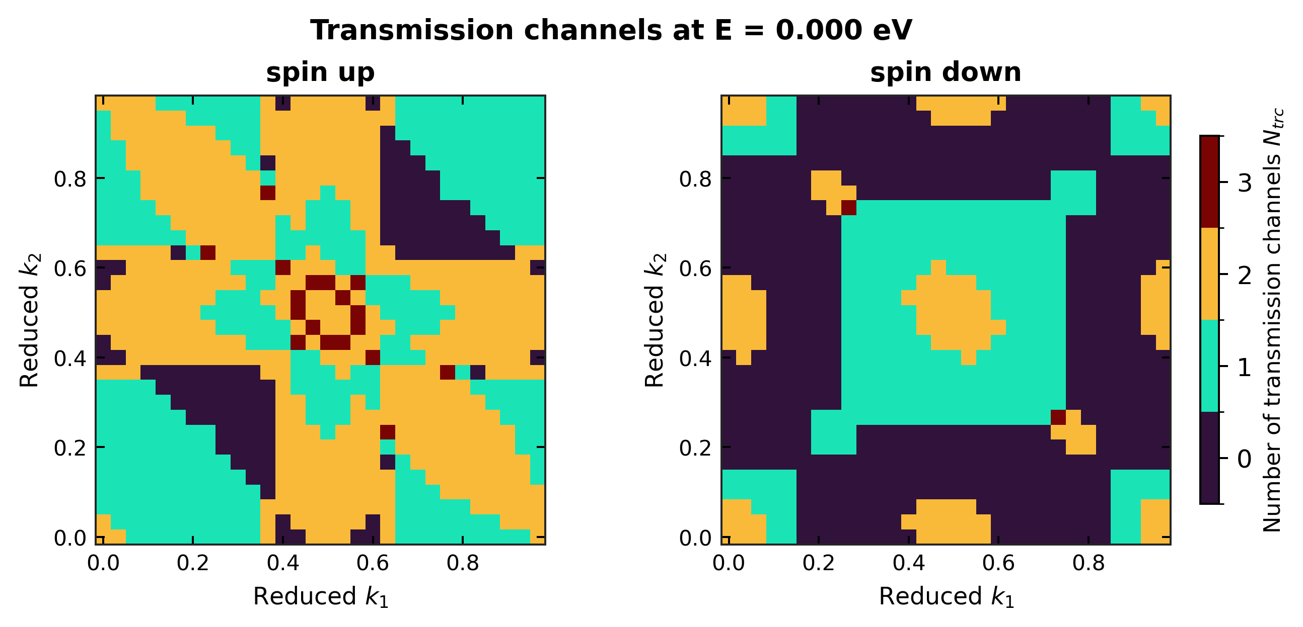
Fig. 2.3.2 NanoDCAL transmission-channel count at the Fermi level for 900 transverse k-points. Separate spin panels preserve the two-dimensional k-space structure instead of flattening it into a sample-index curve.
2.4. How to read and validate the channel map
Each pixel represents one transverse (k1, k2) point at E - EF = 0 eV;
the colour gives the number of open transmission channels at that point. Both
spin panels use the same colour limits, so their different k-space patterns can
be compared directly. The map is not, by itself, a total conductance: a scalar
transport value also requires the transverse-k weights and the appropriate
energy or bias integration.
Before interpreting the spin contrast, check that:
the bcc Fe SCF calculation converged to the intended magnetic state;
both panels use the same energy, transverse mesh, and colour scale;
the channel pattern and any integrated transport quantity are stable when the transverse mesh is refined beyond the illustrated 30 by 30 grid; and
the lead and device calculations use compatible cells, basis data, and spin settings.
Use figures/transmission_channels.png in the generated HTML report and the
SVG or PDF export when editing a manuscript. The matching
results/figure_manifest.json entry records TransmissionChannel.mat as
the source and lists the PNG, SVG, and PDF paths, dimensions, and DPI.
2.5. Going further: quantum transport
The same one-line pattern drives full two-probe transport calculations — LatticeMind builds the lead-SCF → device-SCF → property chain automatically:
Using NanoDCAL, run a transmission calculation along z for a homogeneous
aluminum two-probe device.
Start with the zero-bias transmission and inspect Transmission.mat before
requesting a bias sweep. A useful follow-up is:
Using NanoDCAL, calculate an I-V curve along z for a homogeneous aluminum
two-probe device from -0.2 V to 0.2 V.
For every transport comparison, keep the device geometry, lead construction, NeutralAtomDatabase basis, transverse k-grid, energy grid, and electronic temperature fixed unless the prompt explicitly studies one of those choices.
See NanoDCAL support for the complete list of supported transport, electronic-structure, phonon, and mechanical calculations.
2.6. Three useful follow-up checks
The following prompts exercise different NanoDCAL output families without changing the installation:
Using NanoDCAL, calculate total energy, effective potential, electron
density, and charge analysis for rocksalt MgO.
This producesTotalEnergy.mat,EffectivePotential.mat,TotalElectronDensity.mat, andCharge.matafter one SCF calculation.Using NanoDCAL, calculate the effective mass for GaAs.This producesEffectiveMass.matand tests the electron/hole dispersion fit and directional masses in units of \(m_e\).Using NanoDCAL, run a conductance calculation along z for a homogeneous aluminum two-probe device.This exercises the lead-SCF, device-SCF, and conductance chain and producesConductanceAndCurrent.mat.
For each project, inspect /launch-preview before execution. After execution,
confirm that calculation_status.json.instances marks every requested deck as
succeeded, that the expected .mat files exist, and that
results/analysis_summary.json.warnings contains no unexplained parser or
physics warning. To test only the updated plotting path, ask LatticeMind to
reprocess the existing NanoDCAL outputs without rerunning the solver.
2.7. What you learned
Selecting NanoDCAL is as simple as saying so in your prompt.
LatticeMind handles NanoDCAL’s basis staging, multi-step dependencies, and device chains for you.
Plot-capable results produce a 360 dpi PNG for
report.htmlplus SVG and PDF manuscript exports underfigures/.results/analysis_summary.jsonstores numeric summaries andresults/figure_manifest.jsonlinks each figure to its NanoDCAL.matsource file.