1. Silicon: SCF, band structure & DOS
This is the “hello world” of LatticeMind. In one prompt you will compute the electronic ground state of bulk silicon, its band structure, and its density of states — and get plots and a report. It is the ideal first project.
What you need
LatticeMind installed with an API key (Connecting your AI model). To run the calculation you also need the RESCU solver and a license (Licenses and solver executables); without them you can still follow every step up to execution.
1.1. The prompt
Start LatticeMind (latticemind or latticemind-web) and type:
Do an SCF, band structure, and DOS calculation for silicon, and plot the
band structure and DOS.
That is the entire input. You do not specify the lattice constant, the k-point grid, the functional, or any RESCU keyword — LatticeMind fills those in.
1.2. What LatticeMind does
LatticeMind moves through its pipeline (How LatticeMind works) and reports each stage as it goes:
Plans a three-step workflow:
SCF→BAND-STRUCTURE→DOS, with both post-SCF steps depending on the converged SCF density.Builds the diamond-cubic silicon cell (two atoms, lattice constant 5.43 Å).
Chooses parameters: the PBE (GGA) functional, a
12×12×12k-point grid, and a double-zeta-polarized pseudopotential basis.Renders three input decks and wires the density hand-off from SCF to the band-structure and DOS steps.
Validates the inputs and, when execution is enabled, runs them.
Post-processes the outputs into plots and a report.
1.3. The generated SCF input
LatticeMind writes standard RESCU decks to project_root/inputs/. The SCF
deck it produced for this project — which you can open, keep, and re-run — is:
info.calculationType = 'self-consistent';
info.savepath = './results/scf';
units.length = 'Angstrom';
domain.latvec = [...
    0.0 2.715 2.715;
    2.715 0.0 2.715;
    2.715 2.715 0.0;
];
domain.lowres = 0.5;
atom.fracxyz = [...
    0.0 0.0 0.0;
    0.25 0.25 0.25;
];
atom.element = [1 1];
element(1).species = 'Si';
element(1).path = './pseudopotentials/Si_PBE_TM_DZP.mat';
functional.libxc = true;
functional.list = {'XC_GGA_X_PBE' 'XC_GGA_C_PBE'};
kpoint.gridn = [12 12 12];
option.maxSCFiteration = 100;
Tip
Not happy with a choice? Just say so — “use an 8×8×8 k-grid” or “switch to LDA” — and LatticeMind re-plans and re-renders. You never edit the deck by hand (though you can).
1.4. Running it
Preview and launch:
/launch-preview     # see exactly what will run, and the cost
/execute on         # allow execution
run it
LatticeMind runs the SCF, feeds its density into the band-structure and DOS steps, and then post-processes the results.
1.5. The results
For this project LatticeMind extracted:
Quantity |
Value |
|---|---|
SCF total energy |
−7.8827 Ha |
Integrated electron count |
8.000 e (exactly, an 8-electron cell) |
Band gap (VBM → CBM) |
0.585 eV |
Note
PBE, like all semi-local functionals, underestimates the silicon band gap (experiment ≈ 1.1 eV). The ~0.6 eV result is the expected PBE value — a good sanity check, not an error. For an accurate gap you would use a hybrid functional; just ask LatticeMind for one.
The band structure and density of states are plotted automatically:
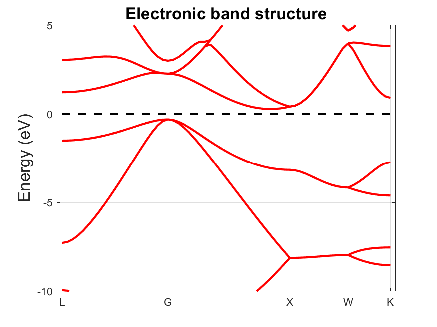
Fig. 1.5.1 Silicon band structure along the high-symmetry k-path, generated by LatticeMind from the one-line prompt.
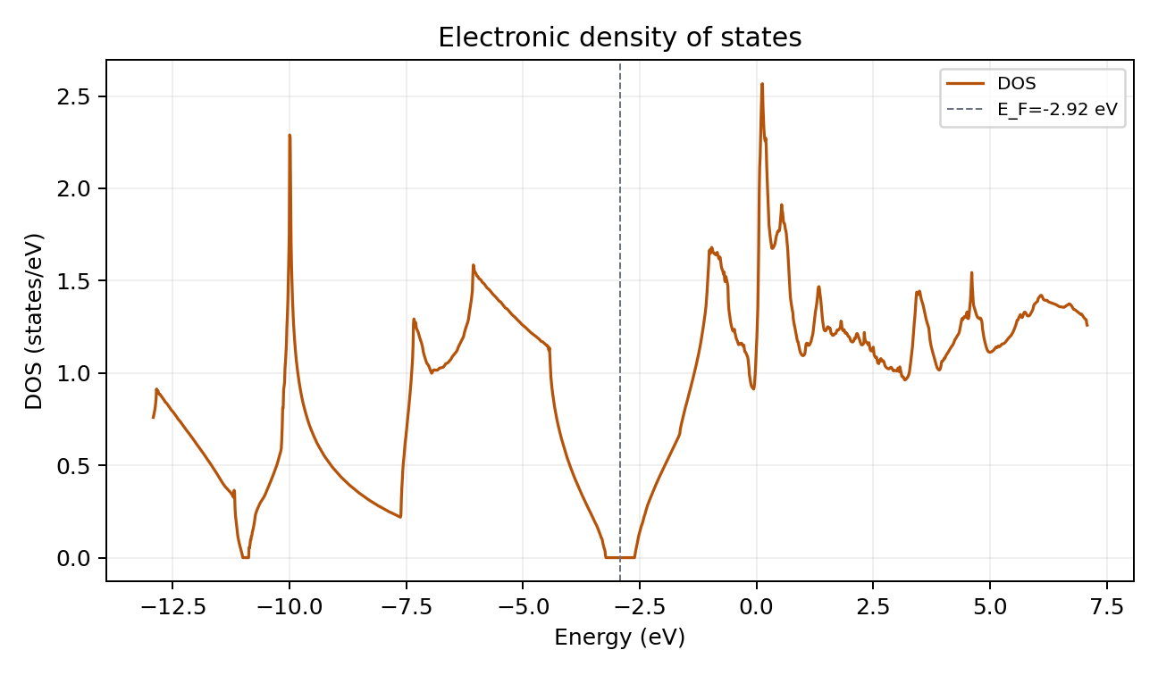
Fig. 1.5.2 Silicon density of states. The Fermi level sits in the gap, as expected for a semiconductor.
1.6. Growing the project, turn by turn
You do not have to ask for everything up front. The same project could have started with just the SCF and band structure, and gained its DOS later:
can you add a dos calculation and plot the dos for the converged density
A continuation reuses the project’s existing plan and whatever is already converged on disk — here, only the DOS actually runs, in well under a minute, and its plot lands beside the band structure. This is the intended way to work: each request builds on the last, completed steps are never recomputed, and a finished run never blocks its own project from continuing.
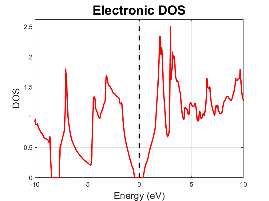
Fig. 1.6.1 The DOS added by the one-line continuation above, computed from the density the SCF step had already saved. The Fermi level sits in the gap.
1.7. Inspecting the project
Everything is on disk in the project folder (Projects & the workspace):
/outputs      # list results, plots, logs, and the report
/plots        # list generated plots
/analysis     # show extracted quantities (energy, gap, electron count)
The generated files include the RESCU decks (inputs/scf.input,
band.input, dos.input), the raw output (results/scf.mat/.h5 and
friends), the plots, and report.html.
1.8. What you learned
A single plain-language prompt produced a correct, multi-step DFT workflow.
LatticeMind chose the structure, functional, k-grid, and basis for you.
The density hand-off between SCF and its dependents was wired automatically.
You got validated inputs, real results, plots, and a report.
Next, plot a III–V band structure in GaAs: band structure along the FCC path, run a k-point convergence study in Aluminium: a k-point convergence study, try a spin-polarized metal in Ferromagnetic nickel: a two-step spin DOS, or an alloy in Building alloys & supercells (SiGe).