2. Band alignment in heterostructures
For quantum dots in semiconductors, a mismatch in band gaps between different materials of a heterostructure very often provides a convenient way to confine electrons or holes along certain directions. As a consequence, band alignment plays a central role in QTCAD simulations.
The total confinement potential energy is given by
where \(V(\mathbf r)\) is the contribution to the confinement potential due to the relevant band edge for electrons or holes (including band bending from gates) and \(V_\mathrm{ext}(\mathbf r)\) is an additional external potential that may be defined by the user, e.g. an impurity potential or a correction to Anderson’s rule (see Custom band alignment).
Anderson’s rule
By default, in QTCAD, bands are aligned using Anderson’s rule [SN81]. This approach is illustrated in Fig. 2.1. According to Anderson’s rule, distinct materials of a heterostructure are first taken to be infinitely separated, in which case their vacuum levels are aligned. The materials are then taken to be brought in contact which each other and equilibrate, in which case their Fermi levels become aligned, forcing the bands to bend at their interface. At a macroscopic scale, this band bending can be calculated by solving the non-linear Poisson equation and may thus be easily obtained with QTCAD.
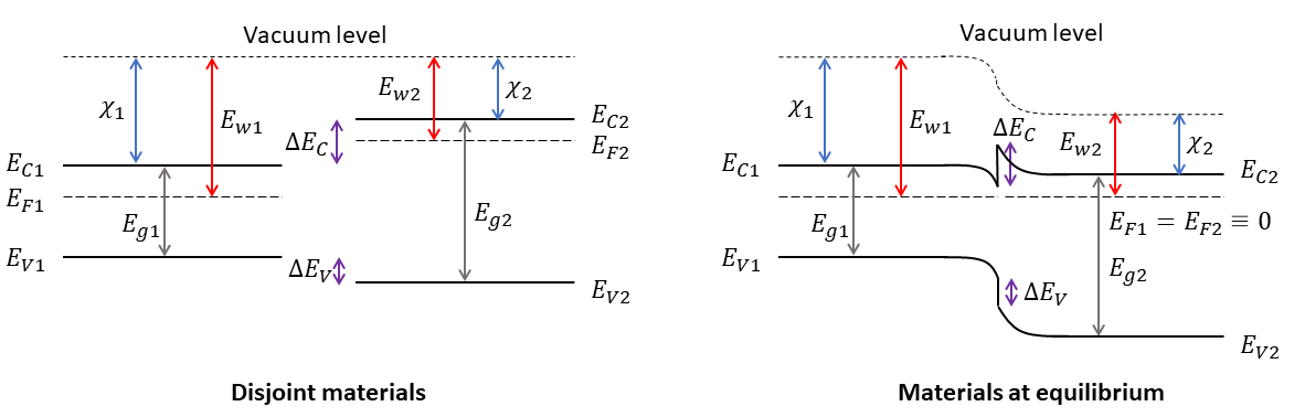
Fig. 2.1 Anderson’s rule for band alignment in semiconductor heterostructures.
In QTCAD, Anderson’s rule is implemented under the following assumptions for the confinement potential.
When the confined charge carriers are electrons, the confinement potential energy contribution arising from bands is given by (see Relationship between electric potential and band edges)
where \(e>0\) is the elementary charge, \(\varphi\) is the electric potential, \(\varphi_F\) is the arbitrary reference potential, and \(\chi\) is the electron affinity of the material at position \(\mathbf r\).
When the confined charge carriers are holes, the contribution from bands is
where \(E_g\) is the band gap of the material at position \(\mathbf r\).
To calculate the confinement potential from bands and store it as the
V attribute of the
Device class, use the
set_V_from_phi
method of this class. The type of confined carrier—electrons ("e")
or holes ("h")—is chosen during the instantiation of the
Device object through the
conf_carriers optional argument. This choice is stored in the
conf_carriers
attribute of the Device object.
By continuity of the electric potential, we have \(\varphi_1 = \varphi_2 = \varphi\) at the interface between the materials. From Eq. (2.2) and Eq. (2.3), this leads to the conditions
The parameters of this equation are visually described in Fig. 2.1. Equation (2.4) constitutes Anderson’s rule.
Custom band alignment
Despite its convenience, Anderson’s rule has several shortcomings.
In particular, electron affinities depend on surface charges and dipoles; however, in a heterojunction, we are interested in properties of an interface between two materials. There is no fundamental reason to believe that those interface properties will lead to the same dipoles as at the interface between a material and vacuum.
As a consequence, in QTCAD, it is possible to modify the confinement potential to include arbitrary corrections to band alignment through Anderson’s rule.
This may be done through two distinct approaches.
By modifying the external potential \(V_\mathrm{ext}(\mathbf r)\) given in Eq. (2.1).
By shifting the value of the reference potential \(\phi_F\) in certain regions of the device.
The first approach only modifies the confinement potential and thus only affects the Schrödinger solver; it has no influence on non-linear Poisson solutions. As a consequence, it cannot truly be seen as a modification of the band structure.
In the second approach, the whole band structure is shifted due to the change in reference potential; this is the approach to be taken if the user wants the classical charge distribution to be modified by the change in band alignment.
Modifying the external confinement potential
By default, \(V_\mathrm{ext}(\mathbf r)\equiv 0 \;\forall\;\mathbf r\). The effect of modifying \(V_\mathrm{ext}(\mathbf r)\) is thus to shift the total confinement potential energy for the confined carrier under consideration with respect to Anderson’s rule.
The \(V_\mathrm{ext}\) parameter corresponds to the attribute
Vext of the
Device class. Modifying this attribute
is conveniently done using the
set_Vext
method of the Device class.
See Parameter setters for more instructions on how to use device parameter
setters.
The total confinement potential \(V_\mathrm{conf}(\mathrm r)\) may,
in turn, be calculated through the
get_Vconf
method of the Device class.
Shifting the reference potential
From Eq. (1.8), we see that shifting the reference potential \(\varphi_F \rightarrow \varphi_F + \delta\varphi\) has the effect of raising the entire band structure by \(e\delta\varphi\). If this is done over certain regions of the device only, then this has the effect of modifying the band alignment of these regions with other regions of the device.
Shifting the reference potential is done using the
add_to_ref_potential
method of the
Device class.
Band alignment from atomistic simulations
In addition to ad hoc modification of the confinement potential, it is possible to use results of atomistic band alignment calculations in QTCAD.
A simple Ab initio method for band alignment calculations was introduced by Dandrea, Duke, and Zunge [DD93, DDZ92]. This method can be applied using Nanoacademic’s powerful, large-scale density-functional theory (DFT) code RESCU+ (see the Band alignment tutorial in the RESCU+ documentation). Here, we describe the theory behind these band alignment calculations, and how they can be input into QTCAD for multiscale heterostructure simulations.
The macroscopic potential
At the atomistic level, band alignment in heterojunctions is determined by the macroscopic potential, which for a material \(\alpha\) with monolayer spacing \(\ell\) (along the direction perpendicular to the heterostructure interfaces, here chosen to be the \(z\) axis) is defined by [DD93, DDZ92]
where \(A_{xy}\) is the area of a two-dimensional unit cell in a plane parallel to the interface and \(V_\mathrm{DFT}(x,y,z)\) is the DFT total potential in the material arising from atomic nuclei, valence electrons, and exchange–correlation.
Multiscale modeling of band alignment
Figure Fig. 2.2 illustrates a typical band diagram in which various materials (A, B, C,…) are stacked together to form a heterojunction; these materials can be metals, semiconductors, or oxides (for the sake of this discussion, oxides can be viewed as semiconductors with larger band gaps). The device is at equilibrium, so that the electron chemical potential \(E_F\) (blue line) is uniform. Since the energy reference is arbitrary, we set \(E_F\equiv0\). The device may be studied at two distinct scales: interfaces may be simulated at an atomistic scale, e.g. with RESCU+, while the mesoscopic regions between the interfaces may be simulated using QTCAD’s non-linear Poisson solver. The conduction and valence band edges \(E_C\) and \(E_V\) are shown for each semiconductor using black horizontal lines at interfaces. The diagram also illustrates the macroscopic potential \(V_\mathrm{macro}(z)\) in red, which is used in DFT calculations to set the relative position of band edges at interfaces (see below). Between these interfaces, \(E_C\), \(E_V\), and \(V_\mathrm{macro}(z)\) are shown as dashed lines, illustrating band bending.

Fig. 2.2 Typical band diagram of a heterostructure. \(E_C\) and \(E_V\) are the conduction and valence band edges, respectively, while \(E_F\equiv0\) is the electron chemical potential. The macroscopic potential \(V_\mathrm{macro}(z)\) is also illustrated in red. Vertical dotted lines represent interfaces between materials. The dashed lines used to represent \(E_C\), \(E_V\), and \(V_\mathrm{macro}(z)\) between material interfaces indicate mesoscopic scale, at which QTCAD is used to calculate band bending. Near interfaces (solid lines), atomistic simulations are used to calculate band offsets.
The procedure to obtain a band diagram using a multiscale approach is the following. The position of the valence band edges with respect to the macroscopic potential in the bulk is calculated for each semiconductor using RESCU+. Following these bulk calculations, macroscopic potential differences are obtained at each interface between semiconductors, enabling to align their bands from first principles. The band diagrams between these interfaces are then calculated at a mesoscopic scale by solving the non-linear Poisson equation. Interfaces between semiconductors and metals are then captured by boundary conditions in which the macroscopic potential relative to chemical potential appears as a parameter that can be calculated from first principles.
Relationship between band edges and macroscopic potential
We first consider interfaces between two semiconductors \(\alpha\) and \(\beta\). We consider the difference between the macroscopic potential at points lying within each material at a distance large from the interface at an atomic scale but small at the mesoscopic scale over which band bending occurs (typically a few nanometers). This potential difference is
where \(V_\alpha^{(\alpha\beta)}\) is the macroscopic potential in material \(\alpha\) neighboring the interface (in the sense described above) between materials \(\alpha\) and \(\beta\). This macroscopic potential difference can be calculated using RESCU+ by simulating the interface using a supercell large enough for \(V_\mathrm{macro}(z)\) to become approximately flat on each side of the interface; the difference between these flat values of \(V_\mathrm{macro}(z)\) then gives \(\Delta V_{\alpha\beta}\) [DDZ92].
Throughout the device, the valence and conduction band edges are related to the macroscopic potential by
where the index \(\alpha\) indicates that \(z\) is in material \(\alpha\), \(E_g^\alpha\) is the band gap energy, and \(\delta E_V^\alpha\) is the difference between the valence band edge and the macroscopic potential in the bulk (for a homogeneous material \(\alpha\)). While \(\delta E_V^\alpha\) may be calculated accurately using RESCU+, \(E_g^\alpha\) may easily be taken from experimental data.
To calculate band bending in mesoscopic regions between interfaces, the macroscopic potential is related to the electric potential \(\varphi\) through
where \(e>0\) is the elementary charge, and \(\varphi_0^\alpha\) is a material-dependent constant that enables continuity of \(\varphi\). Indeed, at a mesoscopic scale, \(V_\mathrm{macro}(z)\) is discontinuous because of the sharp changes described above; at an interface between two semiconductors \(\alpha\) and \(\beta\), this results in a macroscopic potential difference
Continuity of \(\varphi\) at a mesoscopic level is necessary to avoid divergent electric fields \(\mathbf E=-\nabla \varphi\).
From Eq. (2.9), we see that the variations in \(\varphi_0^\alpha\) between materials are set by interface physics and can be calculated with RESCU+. However, the global absolute scale of these constants is arbitrary; indeed, according to Eq. (2.8) any constant shift \(\varphi_0^\alpha\rightarrow \varphi_0^\alpha+\delta\varphi\;\forall\;\alpha\) may be compensated by a corresponding gauge transformation \(\varphi\rightarrow\varphi+\delta\varphi\) without changing the macroscopic potentials. This implies that we may arbitrarily choose the potential value \(\varphi_0^\alpha\equiv\varphi_0^\mathrm{ref}\) in a reference semiconductor, and express all values of \(\varphi_0^\alpha\) for arbitrary \(\alpha\) relative to this reference:
where we have used Eq. (2.9). Substituting in Eq. (2.8), this gives
where \(\Delta V_\alpha\equiv \Delta V_{\alpha,\mathrm{ref}}\). Finally, substituting in Eq. (2.7) results in expressions for the band edges as a function of electric potential
Apart from \(\varphi\), all the quantities appearing above may be calculated from first principles using RESCU+ (\(\Delta V_\alpha\), \(\delta E_\mathrm V^\alpha\)), are known from experiment (\(E_\mathrm g\)), or are arbitrary (\(\varphi_0^\mathrm{ref}\)). In addition, provided that \(\varphi\) is continuous, Eq. (2.11) is completely consistent with the microscopic expression of the valence and conduction band offsets derived in Ref. [DDZ92]. Thus, solving for \(\varphi\) using QTCAD’s non-linear Poisson solver gives us access to the band diagram throughout the entire device at the mesoscopic scale.
Relationship with QTCAD inputs
We now relate the above results with standard inputs of the QTCAD code.
Equating Eq. (2.2) and (2.3) with the equivalent expressions in (2.11), we arrive at
From Eq. (2.12), we arrive at two important conclusions.
A microscopic treatment of interfaces will generically yield a reference potential \(\varphi_F\) that is material-dependent. In fact, equating \(\varphi_F\) given by Eq. (2.12) for distinct materials directly leads to Anderson’s rule.
Substituting (2.12) into (1.8) for the band edges and into the expressions for the boundary conditions (Boundary Conditions), band offsets calculated from RESCU+ atomistic simulations may be directly accounted for.
As a consequence, QTCAD Device and
Material objects
contain two attributes corresponding to \(\delta E^\alpha_\mathrm V\)
and \(\Delta V_\alpha\), respectively:
vlnce_band_macro
and
macro_diff.
The Device attributes are automatically
loaded from the relevant Material
objects when creating regions. However, these quantities are not accounted
for in the reference potential \(\phi_F\) until the
align_bands
method is called with the chosen reference material as its argument
(the choice of reference material sets
\(\varphi_0^\mathrm{ref}\equiv E_w/e\) with \(E_w\) being the work
function of the reference material).
Before calling align_bands,
bands are aligned using Anderson’s rule. After calling this method,
they are aligned in a way that accounts for atomistic parameters.
Note that this method should be called after defining regions but before
setting boundary conditions since these conditions also depend on band
alignment. If align_bands
is not called, or if
align_bands is called but
at least one material in the system does not have
vlnce_band_macro
and
macro_diff attributes,
then the standard approach (Anderson’s rule) is used.
Note
When using the atomistic approach, there is a priori no universal reference material that can be used to build a band alignment database because band alignment is determined by dipoles forming between materials in contact with each other. There is no reason to believe that, say, in a junction of three materials A/B/C, the difference in macroscopic potentials between A and C will be the same as in a single junction A/C because interface physics between A/B, B/C and A/C may lack a common reference (in Anderson’s rule this common reference artificially arises from vacuum).
As a consequence, in QTCAD’s default
materials module, macroscopic potential
parameters have only been coded in GaAs and AlGaAs materials so that they
can be used in tutorials involving GaAs/AlGaAs heterostructures. For any
other heterostructure, users are invited to use band alignment parameters
from the literature or to perform their own calculations with RESCU+, and
input the results in their own
Material
objects.
Relevant device attributes
Parameter |
Symbol |
QTCAD name |
Unit |
Default |
Setters |
Confinement potential from bands |
\(V\) |
|
J |
0 |
|
External confinement potential |
\(V_\mathrm{ext}\) |
|
J |
0 |
|
Reference potential |
\(\varphi_F\) |
|
V |
See note |
|
Electron affinity |
\(\chi\) |
|
J |
4.05 eV |
Through |
Band gap |
\(E_g\) |
|
J |
1.12 eV |
Through |
Valence band from macro potential |
\(\delta E_V\) |
|
J |
0 |
Through |
Macro potential vs reference |
\(\Delta V\) |
|
J |
0 |
Through |
Note
The default reference potential is the silicon work function at the device temperature.
Special care must be taken when defining device parameters using setters.
Device attribute setters (such as
align_bands)
must be called before setting boundary conditions,
because these attributes may enter the formulas used to calculate boundary
values