3. Schrödinger solvers
Two of the most important features of QTCAD are its Schrödinger equation solvers for electrons and holes. These solvers compute the single-particle eigenspectra, i.e. the eigenenergies and eigenfunctions of the system.
There are three main purposes in using the single-particle Schrödinger solvers:
Determining if a given nanostructure hosts bound states (for example, see the Band alignment in heterostructures tutorial).
Calculating the lever arm of certain gates on the electronic structure of a quantum dot.
Providing a basis set for the Many-body solver, which is, in turn, used in master equation simulations to model transport in the sequential tunneling regime.
Both for electrons and holes, we assume the envelope-function approximation (EFA) [Win03]. In a nutshell, the EFA relies on the existence of a separation of lengthscales between the fast-varying atomistic potential and a slow-varying confinement potential set by the nanostructure (heterostructure stack, potentials from electrostatic gates, etc.). Under this approximation, atomic-scale oscillations are averaged out, leading to effective Schrödinger’s equations at the mesoscopic scale. Materials physics then manifests itself through the effective Hamiltonian to be solved and through the parameters appearing therein (e.g. the effective mass tensor or \(\mathbf k \cdot \mathbf p\) parameters, as will be described below).
Differential equations
In QTCAD, Schrödinger’s equation is solved either for electrons or for holes.
This is determined by the value of the conf_carriers attribute of the
Device class, which is "e" for
electrons and "h" for holes.
Effective Schrödinger equation for electrons
For electrons, QTCAD employs the effective-mass approximation. Assuming a single quadratic band, the envelope functions \(F(\mathbf r)\) (also called eigenfunctions) and eigenenergies \(E\) are the solutions of the effective Schrödinger equation
where \(V_\mathrm{conf}(\mathbf r)\) is the total confinement potential including the conduction band edge and possibly additional user-defined potentials (see Band alignment in heterostructures), \(\hbar\) is the reduced Planck constant, \(\mathbf M^{-1}_e\) is the electron inverse effective mass tensor, and \(\mathbf k \equiv -i\nabla\) is the wave vector operator. Envelope functions play the same role as wavefunctions in the usual Schrödinger equation; however, they are not the full solution of the problem since they do not contain atomistic oscillatory components arising from the crystal potential.
Eq. (3.1) is appropriate for conduction electrons in semiconductors like GaAs or AlGaAs, which have a single conduction band minimum at the \(\Gamma\) point (see Fig. 3.3).
In semiconductors like Si or Ge, there are multiple degenerate conduction band minima (called valleys, see Fig. 3.3), in which case Eq. (3.1) is only valid if valley degeneracy is lifted, e.g. under a combination of strongly anisotropic quantum confinement, sharp potentials at interfaces, or strain. In the presence of valley degeneracy, for these materials, it may be more appropriate to use the Multivalley effective-mass theory solver.
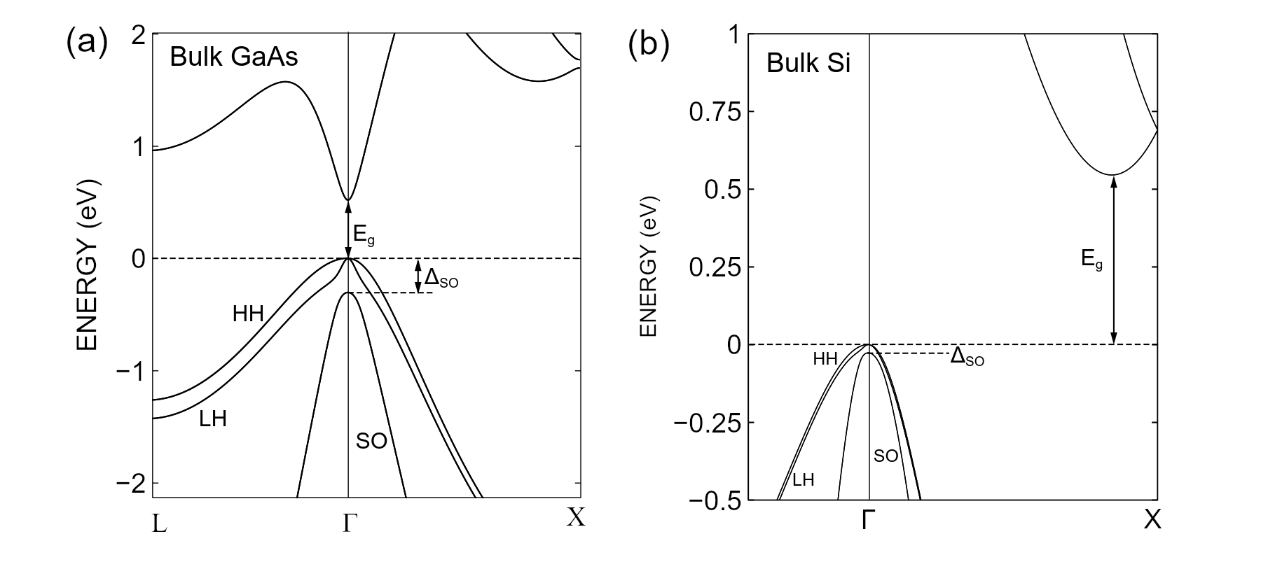
Fig. 3.3 Typical semiconductor band structures with diamond or zincblende lattices. (a) Band structure of gallium arsenide (GaAs). The conduction band minimum is nearly isotropic and centered at the \(\Gamma\) point, making the band gap direct. (b) Band structure of silicon (Si). There are six equivalent conduction-band minima located away from the \(\Gamma\) point along the \(\pm \mathbf{\hat x}\), \(\pm \mathbf{\hat y}\), and \(\pm \mathbf{\hat z}\) directions, at roughly 85 % of the distance between the \(\Gamma\) point and the zone boundary (only the X point is shown above). In both GaAs and Si, the valence band is degenerate at the \(\Gamma\) point, with heavy-hole (HH) and light-hole (LH) bands having equal energy at \(\mathbf k = 0\). In addition, the spin–orbit or split-off band (SO) lies near below the HH and LH bands, and can play a significant role in hole physics. The band structures were calculated using Nanoacademic’s atomistic simulation software NanoDCAL (see e.g. the NanoDCAL tutorial on Spin–orbit interaction). Similar calculations can also be done with RESCU and RESCU+. The band structures were calculated using the local density approximation (LDA), which correctly predicts numerous properties of crystals but underestimates band gaps.
Effective Schrödinger equation for holes
QTCAD convention for holes
We start here by setting the convention we use for holes in QTCAD. Consider the Hamiltonian, \(H_{e}(\mathbf k, \mathbf J)\), for the valence band of a semiconductor. This Hamiltonian depends on the electron momentum, \(\mathbf k\), and the pseudospin, \(\mathbf J\) (which is used to represent multiple bands). The valence band has negative curvature at the band maximum, and accordingly, the electrons occupying the valence band have a negative effective mass, \(m_e^{\ast} < 0\). The total energy of the system can be computed by adding up the energies of all the electrons occupying the valence band. These energies are obtained by diagonalizing \(H_{e}(\mathbf k, \mathbf J)\). Alternatively, if the valence band is almost completely occupied, we can consider a full valence band with energy \(E_{\mathrm{VB}}\) and subtract off the energies of the missing electrons (here we are modelling systems composed entirely of valence-band electrons). This amounts to diagonalizing the Hamiltonian \(E_{\mathrm{VB}} - H_{e}(\mathbf k, \mathbf J)\). We note that removing an electron with momentum \(\mathbf k\) and pseudospin \(\mathbf J\) from a full valence band leaves behind a crystal with net momentum \(-\mathbf k\) and net pseudospin \(-\mathbf J\). We therefore choose a description for holes that aligns with the properties of the crystal. In this sense, the Hamiltonian diagonalized by the QTCAD Schrödinger solver for holes is \(H(\mathbf{k}, \mathbf{J}) = -H_{e}(-\mathbf{k}, -\mathbf{J})\), where we have suppressed the constant energy \(E_{\mathrm{VB}}\) since it has no influence on the eigenstates nor their dynamics. Under this convention, holes are treated as particles with positive effective masses, \(m^{\ast} = -m_e^{\ast} > 0\), and positive charge, \(e > 0\).
Below, we give explicit expressions for the hole Hamiltonian considered in QTCAD. We focus on crystals with a zincblende or diamond lattice, such as GaAs, AlAs, Si, and Ge. The Hamiltonians for holes in these systems are written in the basis chosen in [For93], namely
The states \(\left|\frac{3}{2}, m_J\right\rangle\), with \(m_J = \pm \frac{3}{2}, \pm \frac{1}{2}\), transform like states of total angular momentum \(\frac{3}{2}\) and angular momentum along the \(z\) axis \(m_J\), under the symmetry operations of the crystal. Accordingly, the states \(|\alpha, \sigma\rangle\), where \(\alpha = X, Y, Z\) and \(\sigma = \uparrow, \downarrow\), transform like the coordinate \(\alpha\) and the spin \(\sigma\) under the same symmetry operations. The spin-\(\frac{3}{2}\) matrices corresponding to this basis [with the ordering given above in (3.2)] are given by
Note
Another widely used basis is obtained from the basis in Eq. (3.2) by: \(\left|\frac{3}{2}, \frac{3}{2}\right\rangle \rightarrow -\left|\frac{3}{2}, \frac{3}{2}\right\rangle\), \(\left|\frac{3}{2}, -\frac{3}{2}\right\rangle \rightarrow \left|\frac{3}{2}, -\frac{3}{2}\right\rangle\), \(\left|\frac{3}{2}, \frac{1}{2}\right\rangle \rightarrow -\left|\frac{3}{2}, \frac{1}{2}\right\rangle\), and \(\left|\frac{3}{2}, -\frac{1}{2}\right\rangle \rightarrow -\left|\frac{3}{2}, -\frac{1}{2}\right\rangle\). This leads to Hamiltonians where the first, third, and fourth columns and rows are multiplied by -1. See, e.g., Ref. [Win03] and Ref. [TMW+21].
Schrödinger equation
The physics of holes is predominantly determined by the valence band maximum. In all semiconductors with a diamond or zincblende lattice, the valence band is degenerate or nearly degenerate at the \(\Gamma\) point, which is valence band maximum in such semiconductors. In this situation, a single envelope function does not suffice to describe the system. Instead, the full solution \(\psi(\mathbf r)\) is given by a linear combination of envelope functions for each degenerate band \(n\) [LK55]
where \(u_n(\mathbf r)\) is the Bloch function for band \(n\) evaluated at the \(\Gamma\) point, and \(F_n(\mathbf r)\) is the envelope function for band \(n\). While the \(u_n(\mathbf r)\) have lattice periodicity, the envelope functions vary over a much longer lengthscale determined by quantum confinement in the nanostructure. In general, for any set of quadratic bands, these envelope functions are obtained by solving \(N_\mathrm{bands}\) coupled effective Schrödinger equations [LK55]
for \(n\;\in\;\{1,2,...,N_\mathrm{bands}\}\). In Eq. (3.5), \(\mathbf k \equiv -i\nabla\) is the wave vector operator and \(\mathbf D\) is a \(3\times 3\times N_\mathrm{bands} \times N_\mathrm{bands}\) matrix called the \(\mathbf D\)-matrix. In Eq. (3.5), the \(\alpha\) and \(\beta\) indices run over all Cartesian directions \(x\), \(y\), and \(z\).
The \(\mathbf D\)-matrix term in Eq. (3.5) couples the valence bands together; the interplay between this kinetic energy term and the confinement potential gives rise to several important effects in hole physics, such as lifting of the band degeneracy in nanostructures. Therefore, when simulating holes in QTCAD, the choice of \(\mathbf D\)-matrix bears a significant importance.
k.p module
The kp module contains the following classes:
and the following function:
Defining a \(\mathbf D\)-matrix
The luttinger_kohn_foreman
function defines the \(\mathbf D\)-matrix for the four-band
Luttinger–Kohn model generalized by Foreman to correctly account for
the non-commuting nature of the Luttinger–Kohn parameters in a heterostructure.
The four-band Luttinger–Kohn model may be used to describe materials with zincblende crystal structure. In this model, the two split-off (or spin–orbit) valence bands are neglected, and we concentrate on the two remaining two-fold-degenerate valence bands: the heavy-hole and light-hole bands. Because of the symmetry of the lattice, the Bloch functions corresponding to these bands transform under the symmetries of the crystal like total angular momentum eigenstates, \(|J,m_J\rangle\), with the heavy-hole bands corresponding to \(|\frac32,\pm\frac32\rangle\) and the light-hole bands to \(|\frac32,\pm\frac12\rangle\). In addition, note that in the Foreman generalization of the Luttinger–Kohn model, it is assumed that the growth axis of the heterostructure is the \(z\) axis, and that this heterostructure is grown on a \((001)\)-oriented substrate.
In the above model, neglecting strain, the effective Schrödinger’s equation is [For93]
where we have introduced (\(m_e\) is the bare electron mass)
with
Importantly, apart from the valence band edge \(E_V(\mathbf r)\), the above equations are fully determined by the three Luttinger–Kohn parameters \(\gamma_1\), \(\gamma_2\), and \(\gamma_3\).
The Luttinger–Kohn parameters are material properties. They are defined by
the hole_kp_params
attribute of the Material class,
which is a 1D array containing all the parameters. These parameters are used
when setting up regions of a
Device
to calculate the regions’ \(\mathbf D\)-matrices.
The following code block illustrates how to set up the Schrödinger solver
to use holes, and to specify the \(\mathbf D\)-matrices to be used,
assuming that a
1D,
2D, or
3D Mesh object called mesh has already
been defined:
dvc = Device(mesh, conf_carriers="h")
dvc.hole_kp_model = "luttinger_kohn_foreman"
The first line of code sets the confined carriers to be holes.
The second line of codes specifies which function of the
kp
module must be used when defining the \(\mathbf D\)-matrix for
each region of the device. Here, we use the
luttinger_kohn_foreman
function. Note that this function is open-source in the QTCAD
UI; the user is free to create modified versions of this function to
implement alternative \(\mathbf k\cdot \mathbf p\) models. The
only requirements for such functions are to take a certain number
of Luttinger–Kohn parameters as inputs and output a
\(\mathbf D\)-matrix with the same format as in the
luttinger_kohn_foreman
function.
Note
It is important to specify the nature of the confined carriers and the
hole_kp_model of a Device
object before defining any region of the device. This is because
the nature of the confined carriers and the \(\mathbf D\)-matrix to
be used must be known when creating regions to assign the right
values to the device attributes.
Note
The six-band Luttinger-Kohn model [For93] is also available, however, only for GaAs and Si.
Calculating bulk band structures and density-of-states effective masses
The Schrödinger solver discussed here is appropriate to calculate the energy levels and envelope functions of electrons and holes that are confined in a nanostructure. However, in some circumstances, it may also be relevant to calculate the bulk properties for a given \(\mathbf k\cdot \mathbf p\) model, i.e. the properties of a system with translational invariance along all three Cartesian directions.
For this reason, the kp module contains the definition
of a KPModel class.
The most important attribute of this KPModel
class is the
D attribute, which specifies the
\(\mathbf D\)-matrix for this \(\mathbf k\cdot \mathbf p\) model.
This \(\mathbf D\)-matrix is specified upon instantiation of a
KPModel object. Once this object is
instantiated, it may be used to calculate:
The bulk \(\mathbf k\cdot \mathbf p\) Hamiltonian corresponding to this model for a certain classical wavevector \(\mathbf k\) (see the
hamiltonianmethod).The eigenenergies obtained by diagonalizing this Hamiltonian (see the
energiesmethod). Note that this method may be used to calculate the bulk band structure for theKPModelsimply by looping over a range of \(\mathbf k\) vectors.The angular effective mass of each hole band (see the
angular_effective_massmethod).The density-of-states (DOS) effective mass of each hole band (see the
dos_effective_massmethod).
The last calculation is particularly useful when defining new materials to make sure that the DOS effective masses used to obtain classical hole concentrations in non-linear Poisson calculations are consistent with the \(\mathbf k\cdot \mathbf p\) model that is employed.
Finally, the kp module also contains the
LuttingerKohnModel class,
which is simply a child class of the
KPModel class
which uses the \(\mathbf D\)-matrix calculated from the
luttinger_kohn_foreman method
for the Luttinger–Kohn parameters gamma_1, gamma_2, and gamma_3
specified upon instantiation.
Strain
Until now, we have neglected effects related to strain when solving Schrödinger’s equation. However, strain can be included within effective-mass and \(\mathbf k \cdot \mathbf p\) theory largely thanks to the work of Bir and Pikus [BP74]. The strain on a system is characterized by a strain tensor, \(\varepsilon\), whose components are given by
where \(\mathbf{u}(x, y, z)\) is the displacement field which describes the strain-induced displacement of every point of the structure under consideration, and \(x_i\) is the \(i\)-th component of the position vector, with \(i\;\in\;\{x,y,z\}\).
The strain can be set throughout the device
using the set_strain setter.
The symmetries of the Hamiltonian terms involving the strain tensor can be
obtained by making the following substitution in the models presented above
[see Eqs. (3.1) and (3.5)]
[BP74, STN07]
This idea will be made clearer below through concrete examples.
Typically, strain is included via deformation-potential theory. Under this formalism, the part of the Hamiltonian that depends on strain is given by
where \(\Xi\) represents the deformation potentials, \(\varepsilon\) is the strain tensor, and \(i\) and \(j\) are Cartesian indices.
Electrons
Within QTCAD, electrons are simulated using effective-mass theory. Under this theory, electrons are modelled using a single band/valley. Consequently, the elements \(\Xi_{ij}\) of Eq. (3.11) are scalars. Moreover, because the models we typically consider are characterized by diagonal effective-mass tensors, when making the substitution (3.10) in Eq. (3.1), we find that it requires three parameters to specify the deformation potential [HV56, STN07], each associated to an entry along the diagonal of the effective-mass tensor. Concretely, the conduction-band strain Hamiltonian can be written as
where \(a_i\) are material parameters that specify the deformation potential. The full Schrödinger equation for electrons including strain becomes
In the specific case where the conduction-band minimum is situated at the \(\Gamma\) point, as is the case, e.g., for GaAs, a single parameter \(a_c\) is required to describe the effect of strain [HV56, STN07]
This is consistent with the isotropic nature of the GaAs conduction-band effective mass. In contrast, for materials where the conduction-band minima are along the \([100]\) directions, e.g. Si, the deformation potential, like the effective-mass tensor, requires two independent parameters, \(\Xi_d\) and \(\Xi_u\). Concretely, for the valley in the direction \(\nu\), the deformation potential is represented by [HV56, STN07]
where \((\Xi_d + \Xi_u)\) represents the longitudinal coupling and \(\Xi_d\) represents the transverse coupling.
In QTCAD, conduction band deformation potential parameters are specified using
the
cond_band_def_pot
attribute of the materials making up the device under consideration.
This material attribute is given as a numpy array with three entries
corresponding to \(a_x\), \(a_y\), and \(a_z\) respectively.
For example, we could set the Si
cond_band_def_pot
parameters for the \(\nu = z\) valley via
import numpy as np
import device.materials as mt
import device.constants as ct

Ksi_u = 8.77 * ct.e
Ksi_d = 5 * ct.e
al = Ksi_u + Ksi_d # longitudinal conduction-band deformation potential
at = Ksi_d # transverse conduction-band deformation potential

mt.Si.set_param("cond_band_def_pot", np.array([at, at, al]))
Holes
In a similar fashion, accounting for strain for holes requires making the sustitution (3.10) in Eq. (3.5). Explicitly, the deformation potential terms are given by [BP74]
where \(a_v\), \(b\), and \(d\) are deformation potential parameters and \(\mathbf J\) is the vector of spin-\(\frac{3}{2}\) matrices. In Eq. (3.3), we have written the spin-\(\frac{3}{2}\) matrices in the basis of states that transform like joint eigenstates of \(J^2\) and \(J_z\) in the following order: \(\{\left|\frac{3}{2},\frac{3}{2}\right\rangle,\)\(\left|\frac{3}{2},-\frac{3}{2}\right\rangle,\) \(\left|\frac{3}{2},\frac{1}{2}\right\rangle,\)\(\left|\frac{3}{2},-\frac{1}{2}\right\rangle\}\).
Provided the strain tensor is symmetric (\(\varepsilon_{ij} = \varepsilon_{ji}\)), the strain Hamiltonian is given by [STN07, TMW+21]
with
which correspond to Eqs. (3.6) and
(3.7) above.
The valence-band deformation potential parameters are specified using the
vlnce_band_def_pot
attribute of the materials making up the device under consideration.
This material attribute is given as a numpy array with three entries
corresponding to \(a_v\), \(b\), and \(d\) respectively.
For example, we could set the GaAs
vlnce_band_def_pot
parameters via
import numpy as np
import device.materials as mt
import device.constants as ct

av = 1.16 * ct.e
b = -2.0 * ct.e
d = -4.8 * ct.e

mt.GaAs.set_param("vlnce_band_def_pot", np.array([av, b, d]))
The full Schrödinger equation for holes including strain becomes
Note
In addition to the Bir–Pikus strain model described here [Eqs.
(3.17) and
(3.18)], users are free to
experiment with other strain models using the
strain module.
Within this open-source module, new functions which output the deformation
potential, \(\Xi\), can be defined.
These functions should output a 5D numpy array, where the first index runs
over the elements or global nodes of the mesh, the second and third indices
run over the Cartesian coordinates (corresponding to the strain tensor) and
the fourth and fifth indices run over the bands of the model.
By setting the device attribute,
strain_model, to the name of the
created function, QTCAD will model strain using the corresponding deformation
potential.
Spin–orbit coupling
As the name suggests, spin-orbit coupling couples the spin and orbital degrees of freedom of electrons or holes. The orbital degrees of freedom are typically described by the momentum operator \(\mathbf k = -i \mathbf \nabla\). Because spin–orbit coupling requires the breaking of inversion symmetry, it contains terms with odd powers of \(\mathbf k\) [Win03]. In contrast, both effective mass theory [Eq. (3.1)] and \(\mathbf k\cdot \mathbf p\) theory [Eq. (3.5)], as described above, only include terms quadratic in the wavevector \(\mathbf k\).
As of now, QTCAD can treat arbitrary spin–orbit couplings which are linear in \(\mathbf k\). Below, we give more details and discuss limits under which QTCAD can be used to treat spin–orbit couplings which are cubic in \(\mathbf k\).
Linear spin–orbit couplings
Linear spin-orbit couplings are those that contain only terms that are linear in \(k_x\), \(k_y\), and \(k_z\). While the momentum \(\mathbf k\) gives the ‘orbit’ part of the coupling, the ‘spin’ part can be given as a matrix that acts on the spin (band) degree of freedom of the model. In what follows we will describe how the theory developed above changes when we include spin–orbit coupling in a QTCAD simulation. As an example, we consider the following electron spin-orbit coupling:
where \(\alpha\) is the strength of the coupling, \(k_\pm \equiv k_x\pm i k_y\), \(\sigma_{\pm} \equiv (\sigma_x \pm i \sigma_y) / 2\), and the Pauli matrices are given by
Eq. (3.20) can be rewritten in matrix form as
Using the set_soc method of the
Device class, which modifies the
soc attribute, this
spin–orbit coupling can be included in the model solved by QTCAD:
from device.pauli import sigma_x, sigma_y

dvc = Device(mesh)
dvc.set_soc([-alpha * sigma_y, alpha * sigma_x, None])
The argument of the set_soc method
is a list with 3 entries.
Each entry represents the coupling to \(k_x\), \(k_y\), and \(k_z\)
respectively.
Moreover, the entries should be 2D square arrays with dimension equal to the
number of bands in the model.
Here, for electrons, the arrays are \(2 \times 2\) because the indices
run over the spin of the electron.
For holes in the 4-band Luttinger-Kohn-Foreman model, they would be
\(4 \times 4\).
When an entry is None the coupling for the associated \(k\) direction
is neglected [\(k_x\) associated to the first entry (0 in python indexing),
\(k_y\) associated to the second entry (1 in python indexing), and
\(k_z\) associated to the third entry (2 in python indexing)].
In the case of electron calculations, when spin–orbit coupling is included in the simulation, the envelope functions, \(F(\mathbf r)\), get promoted to two-component spinors to account for the spin of the electron. Accordingly, the effective Schrödinger equation for electrons [Eq. (3.1)] is modified and takes on the following form
where \(\mathbf{H}(\mathbf r)\) is now a \(2 \times 2\) Hamiltonian, \(\mathbf{F}(\mathbf r) = [F_{\uparrow}(\mathbf r), F_{\downarrow}(\mathbf r)]^T\) is a two-component envelope spinor, and \(H_\mathrm{SOC}\) is any spin–orbit coupling term that can be included in QTCAD [e.g. the term written explicitly in Eqs. (3.20) and (3.22)].
Cubic spin-orbit couplings
Cubic spin–orbit couplings depend on third powers of \(k_x\), \(k_y\), and \(k_z\) (including combinations where the total power is 3, e.g. \(k_x k_y^2\)). Often in semiconductor nanostructures, there is a direction of strong confinement, typically taken to be \(z\). In other words, the length scale associated with the potential along \(z\), \(L_z\), is much smaller than the length scale associated with the potential along \(x\) and \(y\), \(L_x\) and \(L_y\) respectively (i.e. \(L_z \ll L_x, L_y\)). This strong confinement along \(z\) reduces a general 3D system to an effective quasi-2D system. In such systems, the subbands related to excitations along \(z\) remain practically unoccupied at low temperatures because they are very high in energy. For all intents and purposes, we can assume that all the particles under consideration occupy the lowest energy subband. Moreover, because the confinement along \(z\) is stronger than the in-plane confinement (\(xy\) plane), we have the following relation:
Consequently, when considering terms cubic in \(k\), the ones that have a \(k_z^2\) factor will dominate. Under these conditions, it is possible to approximate the cubic spin–orbit coupling by an effective linear version which can be modeled using QTCAD.
As an example let us consider the following cubic spin–orbit coupling term for holes in the 4-band Luttinger-Kohn-Foreman model [SBPP13]
where we denote half of the anticommutator as \(\{A, B\} = (AB + BA) / 2\), \(\beta\) is the strength of the spin–orbit coupling, and \(\mathbf J\) is the vector of spin-\(\frac{3}{2}\) matrices (see Eqs. (3.3)).
In the quasi-2D limit described above (where \(L_z \ll L_x, L_y\)), all the holes will have the same value of \(\left<k_z^2\right>\) (since they occupy the same subband), and we can replace the \(k_z^2\) operator by \(\left<k_z^2\right>\) in the equation Eq. (3.25). Because the \(\left<k_z^2\right>\) dominates all other quadratic terms, we also neglect all terms that do not contain this factor. The resulting spin–orbit coupling Hamiltonian is [SBPP13]
Since \(\left<k_z^2\right>\) is assumed to be constant, Eq. (3.26) has the same form as a linear spin-orbit coupling. Thus, under the conditions described above, cubic spin-orbit couplings can be well-approximated by effective linear spin-orbit couplings, which can be included in a QTCAD simulation.
Of course, reducing cubic spin–orbit couplings to their linear forms using the
approach described above requires knowing the value of \(\left<k_z^2\right>\).
To facilitate this approach, the Device
class comes equipped with a
get_k_squared method which
can be used to compute \(\left<k_i^2\right>\) for any
\(i \in \{x, y, z\}\) and for any wavefunction stored in the
eigenfunctions attribute of
the Device class:
dvc = Device(mesh)
s = SchrodingerSolver(dvc)
s.solve()
k2 = dvc.get_k_squared(0, [1, 2])
In the above code snippet, a
SchrodingerSolver object is
initialized from using a Device, dvc.
After applying the solve
method, the eigenfunctions of the device are stored in the
eigenfunctions attribute.
The next step is to calculate \(\left<k_i^2\right>\) for the ground state
using the get_k_squared
method, which takes 2 inputs: the first is the state for which we want to
compute \(\left<k_i^2\right>\) and the second is a list of directions, i.e.
values for \(i\).
In this case, k2 will be a list whose first entry will contain
\(\left<k_y^2\right>\) for the ground state and whose second entry will
contain \(\left<k_z^2\right>\) for the ground state.
The spin–orbit coupling from Eq. (3.26) can be included in
the model solved by QTCAD via:
from device.pauli import J_x, J_y

dvc = Device(mesh)
dvc.set_soc([beta * k2[1] * J_x, -beta * k2[1] * J_y, None])
When including spin–orbit coupling for holes, the Schrödinger equation becomes
where \(H_\mathrm{SOC}\) is any spin–orbit coupling that can be included in QTCAD [e.g. the term written explicitly in Eq. (3.26)].
Magnetic effects
Thus far, when describing the Schrödinger equation for electrons and holes, we
have considered situations where the particle under consideration is only
influenced by a potential energy term, \(V_\mathrm{conf}(\mathbf r)\).
There is however an additional way to influence a charged particle confined to
a nanostructure and that is via an applied magnetic field, \(\mathbf B\).
For a Device object, a magnetic field
can be applied using the setter
set_Bfield.
Within QTCAD, magnetic fields can influence the system in two ways:
they couple to the spin degree of freedom via the Zeeman effect
they couple to the orbital degrees of freedom via the minimal coupling Hamiltonian.
These effects are described in more detail below.
Zeeman effect
The Zeeman effect describes the coupling of magnetic fields to the spin degree of freedom of a charged particle. Within the QTCAD framework, the Zeeman effect is implemented differently for electrons and holes.
Electrons
For electrons, the effect can be described by the following term [Win03]
Here, \(\mu_B = \frac{e\hbar}{2m_e}\) is the Bohr magneton (\(e > 0\)
is the electron charge and \(m_e\) is the electron rest mass),
\(g^*\) is the effective electron g-factor in the system under
consideration, and \(\mathbf S\) is the electron spin operator.
The effective electron g-factor, \(g^*\), can be set using the
set_g_star
method of a Device object, or it
can be inferred from the
g_star
attribute of the materials making up the device being simulated
(see the Material class).
The electron spin operator can be written using the Pauli matrices
where the components of the vector of matrices \(\boldsymbol{\sigma}\) are given in Eq. (3.21).
Just like the case when spin–orbit coupling is considered, when the Zeeman effect is included in the simulation, the envelope functions, \(F(\mathbf r)\), get promoted to two-component spinors. Accordingly, the Hamiltonian gets promoted to a \(2 \times 2\) Hamiltonian matrix. The Schrodinger equation becomes
Holes
Within the Luttinger-Kohn formalism, the Zeeman coupling for holes is given by [Lut56, Win03]
Here, \(\kappa\) and \(q\) are material parameters, \(\mathbf J\)
is the vector of spin-\(\frac{3}{2}\) matrices (its components are given in Eq.
(3.3)) and
\(\mathbf {\cal J} = (J_x^3, J_y^3, J_z^3)\).
There are therefore two parameters, \(\kappa\) and \(q\), which
describe the strength of the coupling between the effective hole spin
and the magnetic field.
These parameters are the equivalent of \(g^*\) for holes.
Just like \(g^*\), the parameters \(\kappa\) and \(q\) can be set
in two ways.
The first is to use a setter, which in this case is the
set_hole_zeeman_params
method of a Device object.
This sets the \(\kappa\) and \(q\) parameters to uniform values
throughout the device.
The second is to allow QTCAD to infer the values from an attribute
(hole_Zeeman_params)
of the materials making up the device being simulated
(see the Material class).
When the Zeeman effect is included in a QTCAD hole simulation, the Schrödinger equation being solved is
General considerations
The Zeeman effect is included by default in any calculation where the magnetic
field is set using the
set_Bfield method.
dvc.set_Bfield(B)
Here, dvc is a Device object and the
input B represents the magnetic field.
It can be given as a 1d array in the case of homogeneous magnetic fields, or as
a 2D array in the case where the magnetic field varies in space and is defined
over the global nodes of the mesh. In the first case, array entries correspond
to the \(x\), \(y\), and \(z\) Cartesian components of the magnetic
field. In the second case, the first array dimension corresponds to the global
node index, while the second corresponds to Cartesian directions.
Note
The Zeeman effect can be neglected in a simulation, even when the magnetic
field is set, by setting the device attribute
zeeman to False.
This can be done via the
set_Zeeman setter:
dvc.set_Zeeman(False).
Orbital effects
Besides coupling to the spin via the Zeeman effect, magnetic fields can also couple to the orbital degrees of freedom of a charged particle. The orbital coupling is typically expressed using the magnetic vector potential, \(\mathbf A\). This quantity is defined such that \(\mathbf B = \nabla \times \mathbf A\).
The vector potential associated to a given magnetic field is not unique. There is thus a degree of freedom associated with choosing a specific vector potential. This choice is often referred to as a choice of gauge. For a homogeneous magnetic field, \(\mathbf B = (B_x, B_y, B_z)\), there are two gauges that are typically considered:
the symmetric gauge
the Landau gauge.
The vector potential in the symmetric gauge is written:
where \(\mathbf r_0 = (x_0, y_0, z_0)\) is a position representing a constant offset in the vector potential that has no influence on the magnetic field.
In the Landau gauge,
The vector potential modifies the wave vector operator, \(\mathbf k\), in the Hamiltonian [Eqs. (3.30) and (3.32)] in the following way:
where \(Q\) is the charge of the particle under consideration (\(Q = -e\) for electron and \(Q = e\) for holes, \(e>0\)), and \(\mathbf{A}\) can be any vector potential (including \(\mathbf{A}_L\) and \(\mathbf{A}_S\)) that corresponds to the applied magnetic field, \(\mathbf{B}\).
Note
The spin–orbit–coupling term, \(H_{SOC}\), has a dependence on \(k\) [see Eqs. (3.20) and (3.26)]. Consequently, this term is modified according to Eq. (3.35).
The modification of the momentum operator can have substantial effects on the spectrum and orbital characteristics of system, e.g. through the formation of Landau levels.
In QTCAD, the setter set_Bfield
can be used to specify which gauge to pick for the calculation of the orbital
magnetic effects:
dvc.set_Bfield(B, r0=(0, 0, 0), gauge="symmetric")
In the above code snippet, the gauge kwarg can be used to work with the
"symmetric" [Eq. (3.33)] or the "landau"
[Eq. (3.34)] gauge, and \(\mathbf r_0\) can be specified
with the r0 kwarg.
Note
The orbital magnetic effects will only be included in a calculation if the
magnetic field is constant (B is a 1d array).
Note
The orbital magnetic effects can be neglected in a simulation, even when
the magnetic field is constant, by setting the device attribute
orb_B_effects to False.
This can be done via the
set_orb_B_effects
setter: dvc.set_orb_B_effects(False).
Relevant device attributes
Parameter |
Symbol |
QTCAD name |
Unit |
Default |
Setter |
Confinement potential |
\(V\) |
|
J |
0 |
|
External confinement potential |
\(V_\mathrm{ext}\) |
|
J |
0 |
|
Inverse effective mass tensor |
\(\mathbf M^{-1}_e\) |
|
1/kg |
See below |
Through |
Hole \(\mathbf k\cdot \mathbf p\) model |
– |
|
– |
luttinger_kohn_foreman |
|
Strain |
\(\varepsilon\) |
|
– |
0 |
|
Hole strain model |
– |
|
– |
|
|
Magnetic field |
\(\mathbf{B}\) |
|
T |
0 |
|
Spin–orbit coupling Hamiltonian |
\(H_{SOC}\) |
|
Jm (see below) |
0 |
|
Effective electron g-factor |
\(g^*\) |
|
– |
2 |
|
Hole Zeeman parameters |
\(\kappa\), \(q\) |
|
– |
-0.42, 0.01 |
|
The default inverse effective mass tensor is that of a \(+\mathbf{\hat z}\) valley in silicon: it is the inverse of the following effective mass tensor (in units of \(m_e\))
[[0.19 0. 0. ] [0. 0.19 0. ] [0. 0. 0.916]]
Note
The total confinement potential \(V_\mathrm{conf} (\mathbf r)\) employed by the Schrödinger solver is given by \(V_\mathrm{conf} (\mathbf r) = V(\mathbf r)+V_\mathrm{ext}(\mathbf r)\).
Note
The soc attribute of the
Device class is a list with three
entries.
The entries contain arrays which represent the coupling to \(k_x\),
\(k_y\), and \(k_z\) respectively.
These entries have units of Jm.
However since the \(k_i\) have units of m, the Hamiltonian,
\(H_{SOC}\), has units of J.
Boundary conditions
Perfect insulators (API reference)
In perfect insulators, the envelope functions are set to zero, \(F_n(\mathbf r) \equiv 0\), for all \(\mathbf r\) that belong to the insulator and for all \(n\). Insulators are specified using the string that labels the relevant boundary or region. For example, in a 3D simulation, insulators may be a set of surfaces on the simulation domain boundaries (as in, say, a particle in a box problem), or they may be physical volumes throughout which the user wishes to set the envelope functions to zero (e.g. an oxide in which envelope function penetration is ignored).
Natural boundaries
As for the Poisson solvers, all boundaries at which no specific condition is specified by the user are natural boundaries.
For conduction electrons, the natural boundary condition is
where \(\mathbf{\hat n}\) is the unit vector normal to the surface pointing outside the simulation domain. This corresponds to setting the component of the probability current normal to the boundary to zero.
The generalization of this condition to holes is
where the \(\alpha\;\in\;\{x,y,z\}\) component of the \(\mathbf v_n\) vector is given by
with \(m\in\{1,...,N_\mathrm{bands}\}\) and \(\beta\;\in\;\{x,y,z\}\).